1 Overview
Time division multiplexing is a common method used to improve the efficiency of data transmission in current synchronous communication systems. For example, the second generation mobile communication GSM system, optical synchronization transmission network SDH, etc. are all examples of using time division multiplexing. In the research and development of modern communication equipment, it is often encountered that high-speed backplane communication, multi-protocol interfaces, network management signaling channels, etc. need to process multiple simultaneous communication interface data at the same time. This article introduces a method of using the multi-channel communication control unit inside the MPC8280 processor chip to process multiple synchronous communication interface data.
MPC8280 is a newer member of Freescale's PowerQUICC II product line. It is manufactured using a 0.13 μm process. The power supply voltages of the core and I / O are 1.5 V and 3.3 V, respectively. Compared with the company's MPC8260, MPC8280's manufacturing process and operating frequency have been improved, but because the core voltage has dropped, power consumption has decreased. Moreover, the capacity of DPRAM (dual-port static memory) in the MPC8280 chip has doubled, and PCI and USB have also been added.
The MPC8280 chip is composed of three main functional modules such as the main core, SIU, and CPM, as shown in Figure 1. The main core of the processor of MPC8280 is called G2_LE, which is a multi-stage pipeline superscalar processor of PowerPC architecture. The operating frequency of the MPC8280 core is 16 * 50 MHz. The SIU module is mainly responsible for 60x bus control, PCI bridge and clock generation. The CPM module is responsible for processing communication transactions, that is, processing the SCC, SMC, FCC, MCC, USB, SPI, I2C and other communication control units to send and receive data. The multi-channel HDLC controller described in this article is implemented using the MCC (multi-channel controller) communication control unit under CPM.

The static memory integrated in the MPC8280 includes DPRAM, global configuration registers, and SI RAM (serial interface routing table configuration space). Among them, the first block of 32 KB of data DPRAM space is divided into 16 banks (storage space blocks). In addition to using the global configuration register for the most basic parameter configuration, the communication control unit in the CPM must also use the parameter configuration storage block for further configuration. In general, each communication control unit in the CPM has two parameter configuration storage blocks, and the parameter configuration storage blocks are all located at the designated address in the DPRAM. SI RAM is mainly used to configure the routing table of TSA (Time Slot Distributor).
2 SI (TSA) design
MCC is always used in conjunction with SI (serial interface) (because MCC is only a data processing unit and is not responsible for the interaction between communication data and MPC8280 pins), therefore, only when SI is configured well, the MCC unit can work normally. Each MCC is only associated with one SI, and MCC1 is only allowed to connect to SI1, and MCC2 is only allowed to connect to SI2.
MPC8280 contains 2 SIs, each SI can control up to 4 TDM (Time Division Multiplexing) ports. Each TDM port has its own independent sending and receiving frame synchronization pulses and sending and receiving clock pins. The synchronization edge of the clock, clock multiplication (1 & TImes; or 2 & TImes; clock mode), and the number of leading clock bits of the frame synchronization signal are programmable. The relationship between SI and MCC is shown in Figure 2.
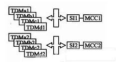
Figure 2 Relationship between SI and MCC
The main work of TSA is data routing, that is, the I / O data of each communication control unit in CPM is transferred to the TDM port in units of bits or bytes. In other words, the TSA is equivalent to the TDMA (Time Division Multiplexing) function module of each communication control unit (MCC, SCC, SMC, FCC, etc.) in the CPM module of the MPC8280. The programming of the TSA is independent of the back-end communication control unit. TSA performs routing based on the routing table constructed by SI RAM.
SI itself has no buffer, and it is directly connected to the FIFO of each communication control unit at the back end; SI is driven by the clock and sends the received frame bit stream to the FIFO of each designated communication control unit according to the configuration of the routing table. And output the data in the FIFO of each designated communication control unit to the pins of the TDM port, and interact with the BD (buffer descriptor) table and interrupt of each communication control unit to complete the communication task.
The programmer completes the construction of the routing table by programming the SI RAM block. Each SI contains 2 SI RAM blocks, which are used to design the routing table for sending and receiving, so that the 2 SI modules inside the MPC8280 contain a total of 4 SI RAM blocks. Each routing table constructed by SI RAM includes 256 entries, each entry is 2 bytes long, and each entry can control up to 8 bytes of serial stream data distribution, so 1 SI module supports The length of the longest frame can reach 256 & TImes; 8 & TImes; 8 = 16 384 bits. The content of the routing table entry is to designate the synchronous data stream with 1 to 8 bits or bytes on the TDM port to be distributed to MCC, SCC, SMC, FCC and other communication control units. The last entry must activate the end tag of the routing table to tell TSA that it has finished processing a frame, please wait for the next frame synchronization signal to arrive.
As shown in Figure 3, each SI RAM (containing 256 entries) is equally divided into 4 banks, that is, each TDM port has one bank to one-to-one correspondence; each bank can be assigned by the programmer as the corresponding Different TDM ports (but it is not allowed to correspond two TDM ports to the same bank). In this way, the serial data stream of the TDM port is sent to the designated communication control unit for processing under the control of the SI RAM entry of the designated bank. The length of a bank can be freely set by the designer (the routing table has the first and last signs), this is because for different applications, the number of bits per frame is not necessarily the same; the routing table accurately determines the frame flow of each TDM port The number of bits. Obviously, how many entries must be processed by a frame stream can also be calculated, that is, the total number of bits in the frame stream / the number of bits processed per entry. Note that the number of entries in the routing table must be an even number, so when programming, if there is really only one entry, then another entry with empty content must be added.
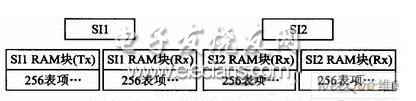
Figure 3 SI RAM block composition and corresponding structure
In addition, because the reception and transmission of the TDM port are controlled by two SI RAM blocks, the allocation of the bit stream sent and received by the TDM port can be arbitrarily designed, even allowing the discontinuity of the bit stream to be allocated to a communication control unit It also allows a communication control unit to receive from one TDM and send from another TDM.
3 MCC standard channel design
The data of an MCC is transmitted on 4 TDM ports controlled by a specific SI; each MCC can support 128 time-division multiplex channels (see Figure 4), used to transmit HDLC, transparent channels, or No. 7 signaling channel data. The design of this article is to use MCC to realize multi-channel HDLC communication protocol. The data flow of MCC can be directly sent to the FIFO of the corresponding channel of MCC through the bridge of TSA. Each MCC can be decomposed into 4 sub-modules, and each sub-module (including 32 channels) corresponds to one TDM port, that is, to process data of different physical TDM ports. The working mode of each channel in the MCC can be set independently, and the transceiver relationship can also be independently mapped; it supports global loopback and independent loopback based on a single channel.
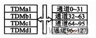
Figure 4 TDM port and MCC channel correspondence
Each MCC contains 128 channels with the same function, each channel has a set of configuration registers, these registers have the same function, and rely on the channel number for index addressing, and then initialize.
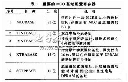
The initialization of MCC follows the order of global first, then channel. The global parameter register of the MCC is located in DPRAM (bank 9) and occupies 128 bytes. The offset of this register group from the base address of DPRAM is 0x8800. The most important address index registers in the global parameter settings that will affect the addressing of the configuration register space of each channel are listed in Table 1.
Each channel has a 64-byte dedicated parameter register. Calculate the base address of the dedicated parameter register group of the specified channel using the "DPRAM base address + 64 x channel number" method.
There are 8 bytes of additional parameter registers for each channel. The base address of the additional parameter register group of the specified channel is calculated using the "DPRAM base address + 8 x channel number" method. The main contents of this block include: TBASE (16 bits, send the BD table first address calculation element); RBASE (16 bits, receive the BD table first address calculation element).
BD tables are usually placed in off-chip memory. One MCC contains 128 channels, and each channel has its own BD table. The BD tables of all 128 channels are continuously stored in a 512 KB segment. The calculation method of addressing the base address of the BD table corresponding to a channel in this space is: MCCBASE + 8 × RBASE (receive), MCCBASE + 8 × TBASE (send). Both the receiving and sending BD tables are in a ring formation. The receiving BD table must contain at least 2 entries, and the sending BD table must contain at least one entry. When programming, construct a structure array, and TBASE and RBASE can be designed as an array index corresponding to the channel number.
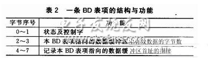
Each BD entry has 8 bytes, as listed in Table 2.
The interrupt table of the ring queue structure is also placed in off-chip memory. The sending interrupt corresponds to a table with a base address of TINTBASE; the receiving interrupt corresponds to 1 to 4 tables with a base address of RINT-BASE0 to RINTBASE3. The length of the interrupt table is completely determined by the user, but at least includes 2 entries. Each interrupt entry is 4 bytes in length, and records whether the interrupt entry is valid, the interrupt flag, and the channel number that triggered the interrupt.
4 MCC super channel mode design
The MCC working in the super channel mode requires SI to use bytes as the routing unit. Through the "super channel" technology, the FIFO that originally belonged to several channels is aggregated into a larger FIF-O, which transmits a large-capacity synchronous data stream. The method of aggregation is to specify the channel number of a few MCCchannels in SI RAM to belong to a super channel, that is to say, in order to make MCC work in super channel mode, the initialization of SI RAM and super channel table must be completed.
The super-channel table is used to indicate which channels of FIFO share the control parameters of the specified channel. For example: 160, 161, 162 and other three standard channels form a super channel, and the control register of channel 160 controls the behavior of the super channel, then fill in "160" in the super channel table entry.
The super channel table is only used for transmission control, and the receiver does not need to construct a super channel table. The programming of the reception is relatively simple, it does not need to set up a super channel, and it is relatively straightforward. The data that needs to be processed by a channel can be opened directly in the SI RAM to receive.
5 Interruption model
MCC's interrupt response uses a two-level interrupt model: the first level is the global interrupt status flag register MCCE, and the second level is the interrupt ring table. MPC8280 * has 5 interrupt ring tables to provide interrupt flag service for MCC channel interrupts: 1 for sending and 4 for receiving. The interrupt ring table is common to all channels. When initializing each channel, you must specify which receive interrupt table it uses to report the receive interrupt. Using this feature, you can design a priority interrupt response mechanism.
Note: Because it is a ring table, the Wrap bit of the last entry in the ring table must be set to 1, and all other entries in the ring table must be set to O.
Whenever an MCC channel triggers an interrupt, the CPM module of the MPC8280 will write an entry to the current empty entry position in the interrupt ring table, and set the "V" valid flag position of the entry to 1, indicating that an interrupt has been received , Waiting for user response and processing. And add 1 to the entry pointer to point to the next empty entry (when the pointer reaches the last entry of the ring table, the CPM module automatically reloads the value of the base address of the interrupted ring table into the entry pointer register to make the CPM the next time The written position is repositioned to the top of the interrupted ring table).
Note: If some masking events are set in the interrupt mask register INTMSK, when these events occur, CPM will not write entries to the interrupt ring table, and naturally will not trigger the global interrupt status flag register MCCE.
The user ISR code responds to the MCC interrupt. When accessing the interrupt ring table entry, the "V" flag should be cleared first, then the specific interrupt request is processed, and the interrupt flag of the MCCE register is cleared before exiting the interrupt service routine. The programmer should decide according to the actual situation of the system whether to exit after processing all interrupt events in the interrupt ring table after entering the MCC interrupt service program, or to exit the interrupt service program only after processing an interrupt request in the interrupt ring table, which requires The programmer makes comprehensive considerations based on the interrupt response time and does not affect the operation of other program code.
6 Actual commissioning
Loopback test is an important means to test whether the communication hardware itself is normal. Each communication processing unit of the MPC8280 itself has a loopback control bit. For example, the loopback control of SCCHDLC is set in the GSMR_L register; the loopback control of a single channel of the MCC is set in SI RAM. A single TDM port can also be self-looping and set in the SIxMR register. Therefore, you can test whether the driver is written correctly by self-looping on a single channel of MCC and self-looping on a single TDM port. In this test, the TDM port of the MPC8280 is driven by the off-chip clock and frame synchronization pulse. Note: Before testing, you must use an oscilloscope to confirm that the frequency and waveform of the clock on the TDM port pins meet the hardware design requirements. In addition, the clock edge relationship between the MPC8280 and the external switching chip should be carefully selected to avoid data synchronization errors caused by abnormal clock synchronization.
After the initialization code is completed, you should use shell tools or other observation methods to check that the initialization code writes to the relevant registers to meet the design goals. Don't get the correct result because of carelessly writing the wrong register value. Because the work of the MCC must be completed with the cooperation of the SI module, the SI module and the MCC can be debugged separately. If there is a driver of the SCC (SMC can also be) communication unit that has been debugged, the data flow of the SCC can be directed from the I / O pin to the SI module, as shown in FIG. 5. Test whether the loopback of the SCC through the SI module is normal, and you can test whether the driver of the SI module is correct. After testing the SI module driver, and then replacing the SCC driver with the MCC driver, you can easily test the MCC driver using the same model. Note that the MCC works in standard mode and super channel mode to initialize the routing table of the SI RAM slightly differently.

Figure 5 SCC1 undergoes loopback test through SI module
7 Summary
MPC8280 is a processor with low power consumption and strong communication processing ability. With the large communication capacity communication capability of the multi-channel controller inside MPC8280, it is relatively easy to design applications such as signaling channels, data channels, and protocol converters. This article introduces the communication principle and debugging method of the multi-channel controller inside the MPC8280, and hopes to help scientific researchers with relevant application needs.
Galvanized aircraft cable
Main construction: 7x7 1/16" to 1/4"
7x19 3/32" to 3/8"
Surface: galvanized, PVC-coated, stainless, balck treated
Packing: 10000ft,5000ft,2500ft per reel or as per customer's request
galv. wire rope, GAC, MIL-83420,Steel Wire Rope,Galvanized Wire Rope,Galvanized Steel Wire Rope,Galvanized Aircraft Cable
ROYAL RANGE INTERNATIONAL TRADING CO., LTD , https://www.royalrangelgs.com