Digital-to-analog converters are used in a wide variety of applications and are often used with amplifiers to condition the output signal. The amplifier can boost output current drive capability, convert differential signals to single-ended output signals, isolate downstream signal paths, or provide complementary bipolar output voltages. Figure 1 shows a typical signal chain for a single supply, consisting of a reference, a digital-to-analog converter, and a buffer. To maintain high dynamic output range and high signal-to-noise ratio performance, digital-to-analog converters (DACs) are typically designed to operate at full swing and the reference voltage (VREF) is set equal to the supply voltage (VDD). This maximizes the use of digital codes. When using a single supply, the DAC and output buffer supplies are typically connected to the same power line. In this configuration, rail-to-rail input and output amplifiers are required.
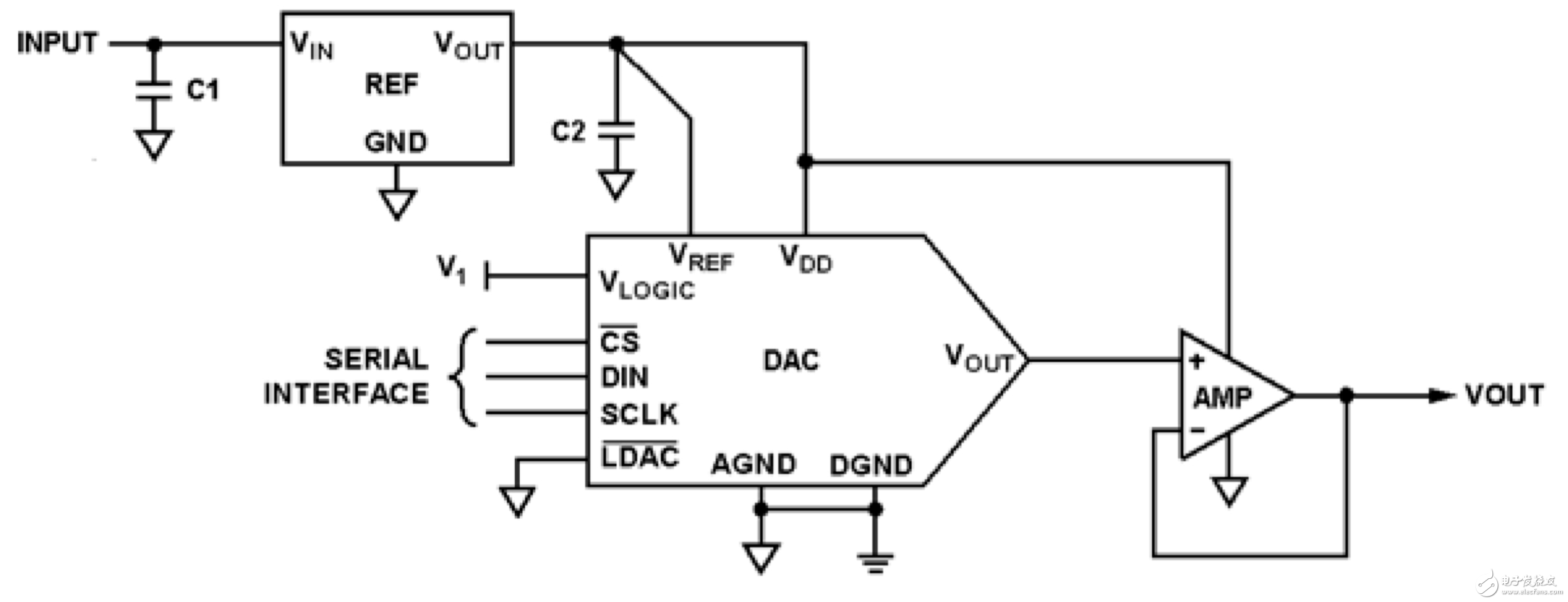
Figure 1: Typical signal chain for single-supply operation
The input stage of a classic non-rail-to-rail input amplifier uses a p-type (or n-type) differential pair. The p-type input amplifier allows the input common-mode voltage to reach and contains a low supply rail. This is especially useful in ground detection applications. On the other hand, n-type input amplifiers allow input voltages ranging from a few V above the low supply rail to high supply rails. These amplifiers are suitable for applications that require high supply rails, such as high-side current-sensing monitors. To extend the input common-mode voltage to two supply rails, the rail-to-rail input amplifier integrates both n-type and p-type input stages.
The main part of the rail-to-rail input amplifier is designed with two parallel input differential pairs, n-type and complementary p-type. Enter the common mode voltage to determine which differential pair is on and active. The p-type differential pair turns on when the input voltage approaches and reaches the low supply rail. For high supply rails and the following input voltages, the n-type differential pair is activated. This topology allows the amplifier to maintain a wide dynamic input voltage range and swing the signal up to two supply rails. However, these amplifiers have a drawback, commonly referred to as "crossover distortion," where input differential pairs often exhibit different offset voltages. When switching from one pair to another due to a change in the input common-mode voltage, a step-like characteristic is produced, which can be seen from the relationship between the offset voltage and the input common-mode voltage. This crossover distortion is inherent in all rail-to-rail input amplifiers with dual differential pair topologies. Figure 2 shows an example. In this example, the amplifier supply is +5V and ground, and the crossover region is at 3.4 V input common-mode voltage. These amplifiers can be used in applications with rail-to-rail input voltage ranges, but can cause problems when the input common-mode voltage is in the transition band. For example, when the amplifier is used as a DAC output buffer, "crossover distortion" can cause nonlinearities.
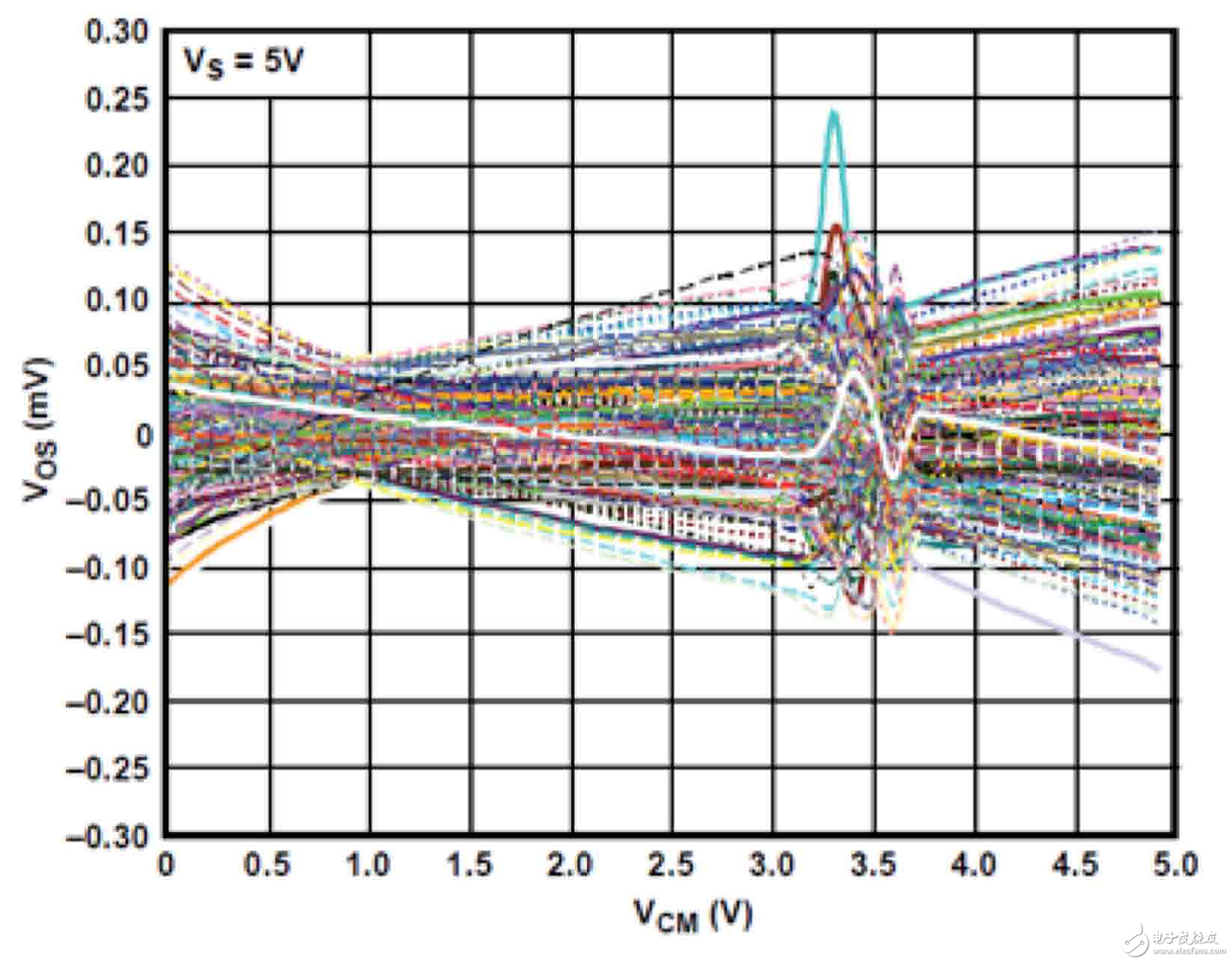
Figure 2: The relationship between the input offset voltage of a typical rail-to-rail input amplifier and the input common-mode voltage
Figure 3 shows the integral nonlinearity (INL) error of a circuit using a 16-bit digital-to-analog converter and a typical rail-to-rail input/output buffer. The INL error is the deviation of the actual converter transfer function from the ideal transfer function, expressed in LSB. Note that the digital-to-analog converter input scans from code 200 to code 216-200, which excludes approximately 15 mV (200 codes) across the range because the rail-to-rail output amplifier does not have full rail-to-rail output. And need to leave some output margin (usually specified in the data sheet). Crossover distortion is detected at roughly 45,000 input digital codes, which is equivalent to a 3.4 V input common mode voltage. Obviously, the amplifier crossover distortion will degrade the INL performance and affect the system accuracy. In this example, for a 16-bit system, the crossover nonlinearity is as high as 4 to 5 LSB. Many systems perform calibrations to eliminate the initial offset voltage, but this nonlinearity cannot be eliminated by calibration.
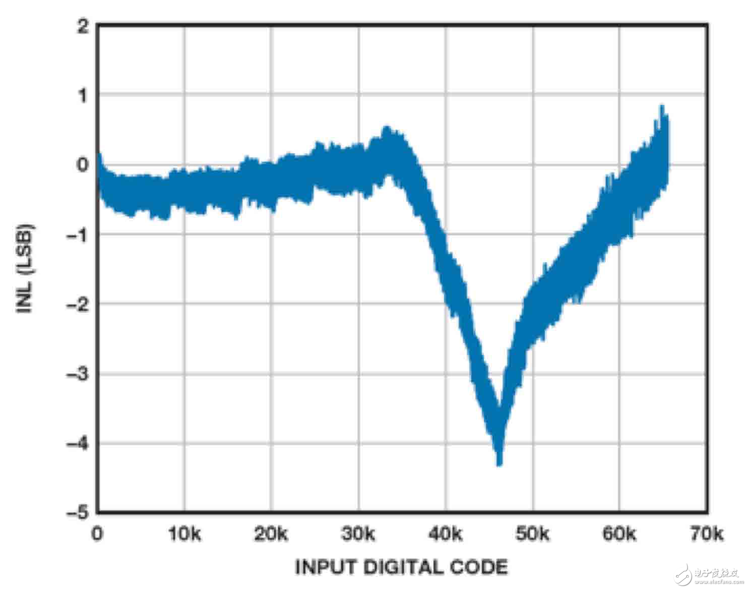
Figure 3: Integral Nonlinearity (INL) for a 16-Bit DAC with a Typical Rail-to-Rail Input Buffer
The crossover nonlinearity problem can be solved using a zero crossover distortion amplifier. This amplifier integrates a charge pump input enhancement circuit on-chip to achieve rail-to-rail input swing. The charge pump boosts the internal supply of several V to provide the headroom required for the input stage, allowing the amplifier to achieve rail-to-rail input swing without the need for a complementary input differential pair. Therefore, it does not have crossover distortion. ADI's ADA4500-2 is such a zero-crossing distortion amplifier. Figure 4 shows the offset voltage of the device versus the input common-mode voltage. It can be seen that the offset voltage is very stable over the entire input common-mode voltage range.
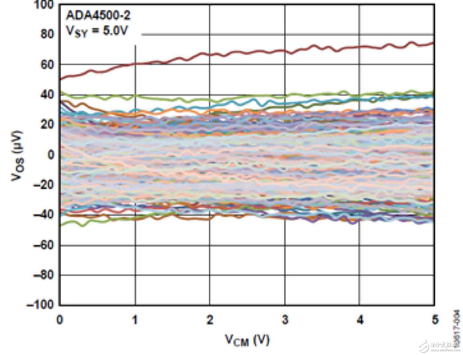
Figure 4: The relationship between the offset voltage of a zero-crossing distortion amplifier and the input common-mode voltage
The use of zero crossover distortion amplifiers eliminates crossover nonlinearities in digital to analog converter systems. Figure 5 shows the circuit INL using the same 16-bit digital-to-analog converter with the ADA4500-2. Zero crossover distortion improves INL performance to less than +/-1 LSB.
An alternative to a distorted amplifier that uses a reference voltage (VREF) below its supply voltage (VDD) as a converter supply can also avoid cross-linearity. For example, use a 5 V supply voltage and a 2.5 V reference. This ensures that the crossover area of ​​a typical rail-to-rail input amplifier is not within the range of the input digital code. But the drawback of this method is that the output range is halved. If the signal level is too low, an external amplifier may be required to amplify the output signal. If the system has multiple power supplies, another possible method is to provide a higher supply voltage to the amplifier, allowing the use of non-rail-to-rail input amplifiers. Increasing the supply voltage will provide enough headroom for the input stage. However, the power efficiency of this method is low.
In summary, it is important to carefully select the appropriate amplifier as the DAC output buffer. You can reduce the DAC reference voltage at the expense of the output range, or increase the buffer supply voltage at the expense of low power performance. Or, better yet, you can use rail-to-rail input/output amplifiers to maximize input and output range, but consider using zero-crossing distortion amplifiers to avoid crossover nonlinearities.
Motor Wire
We supply variety of output lead wire for motor and motor wiring harness. With the properties of chemical erode resistance, excellent bendability in high and low temperature environment and impregnating varnish erode resistance even at 302°F (150°C), this kind of wire also can bear high temperature of 392°F (200°C) with FEP and silicone rubber insulations. All of our wires and cables are UL, RoHS and REACH complaint such as UL1430, UL3266, UL3122 and UL1332 etc.
Motor Wire,Single Phase Motor Wiring,Dc Motor Wiring,Motor Lead Wire
Feyvan Electronics Technology Co., Ltd. , https://www.fv-cable-assembly.com