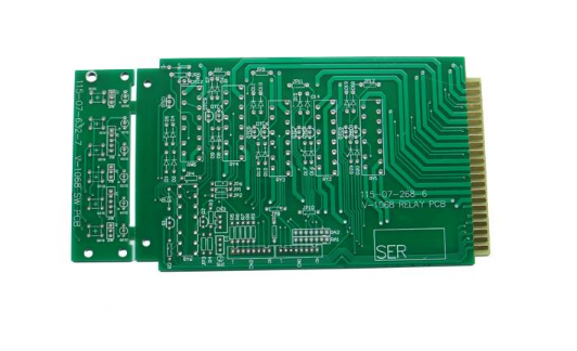
High-frequency questions during the game need to use self-made PCB to improve the circuit's anti-jamming capability. So studied a long time PCB thermal transfer technology. According to this set of procedures that have been repeatedly tried out over the past month, a high-precision PCB with MSP430 chip can be manufactured in a short time, with a line width of 10 mils and a pitch of 8 mils, which can be soldered with a 64-pin chip package. The probability of wire breakage is very low. .
〇, tools and materials used
Altium Designer + home laser printer + heat transfer machine + self-made PCB corrosion tank + blue environmental corrosion agent + laser toner scavenger + small hand drill + glass fiber copper clad laminate (or bakelite).
First, draw the PCB (using Altium Designer)
1000mil = 1 inch = 2.54cm, and the board spacing is 2.54mm = 0.1 inch = 100 mils.
Use patch components as much as possible to reduce the hassle of drilling.
The patch element and the wiring are on the same side, and the in-line element is mounted on the other side.
Because self-made PCBs are well-made, it is difficult to modify them like a universal board, so test points should be properly reserved.
PCB Rules Reference:
Line Width > Width > 15mil (10mil may break during transfer).
The safety clearance Clearance > 10 mil, preferably set to 30mil or more, the spacing is too small to be welded.
Pads: Aperture is set to 20 mils, drilled later as needed (set to 20 mils for easy bit drilling when corroded); diameter > 80 mil, the larger the later the easier it is to drill (if the OD is too small, drill a little The ring pad will break, causing the solder to become weak and the pad to fall off more easily.) For a common 100 mil IC, transistor, etc. pad, if the pad diameter is greater than 100 mil, adjacent pads will be connected, it can generally be set to 85mil.
Copper Plane -> PolygonConnect: Relif Connect, Width Conductor width> 20 mil, Airgap width = 15 mil.
The PCB substrate is set according to the actual size of the copper clad laminate. Generally, a single layer is used. If the self-made double layer board is used, it is relatively difficult to align the two sides.
Second, print
Delete unnecessary layers: Only TopLayer or BottomLayer layers are printed when printing and other layers are deleted.
If it is TopLayer, you should check Mirror.
The pad is printed as a hole (check Hole), so doing the later drilling will be better positioned.
The color is set to black, and the print mode is set to monochrome (ColorSet: Mono).
Print size: ScalePrint 1.0, not FitDocument.
Turn off the printer's ink save mode. For details, see the printer's instructions.
To prevent paper jams from being directly placed on the thermal transfer paper, the thermal transfer paper can be cut and then printed on a plain A4 paper and printed on the smooth side of the thermal transfer paper.
After printing, wait for the thermal transfer paper to cool, and the toner will be fully held in place for transfer.
Third, thermal transfer
The heat transfer machine needs to be warmed up 5 minutes in advance and set to about 180°C.
The copper-clad laminate is first sanded and then cleaned with detergent to remove any invisible oil on the surface. After cleaning, do not touch it with your hands and dry it naturally (preferably do not rub it with paper).
The printed thermal transfer paper is cut to a suitable size and fixed on a copper clad board with heat-resistant paper tape.
Put in the heat transfer machine, heat transfer about 5 times. Slowly remove the thermal transfer paper from one side. If it is not properly transferred, it can be re-transferred several times; if there is a small amount of disconnection, it can be painted with a fine marker (do not use a large area of ​​oily marker to apply, so that later will be difficult to clean). 5. The CCL should be completely cooled before it can corrode, otherwise it is easy to get out of ink.
Fourth, corrosion
The etching tank is filled with an etchant solution, the heating bar is turned on, and the etching solution is heated until the temperature reaches about 50 degrees, generally not exceeding 60 degrees.
Place the completely cooled copper clad laminate in the etching solution.
Turn on the air pump to accelerate the reaction.
Where there is no ink, the color change is seen and the copper foil is etched away to expose the substrate. When the ink has not been corroded, it can be removed. If you put too long, there may be ink from the edge of the place may begin to slowly erosion.
Fifth, remove the ink, clean
Use a brush dipped in alcohol or laser toner remover, brush off the toner, and then rinse with water.
Sixth, further processing
Use an electric drill to drill the hole. Generally, the drill bit with a diameter of about 0.6 mm can be used for the pin. Take care to break the drill. You can use saws for cutting.
Zhejiang Kaimin Electric Co., Ltd. , https://www.ckmineinverter.com