Renesas's RX210 series is a high-performance, low-voltage, ultra-low-power 32-bit RX CPU core-based flash memory mcu. The CPU has 73 basic instructions and 9 DSP instructions. The maximum operating frequency is 50MHz, and the 78DMIPS performance, multiplication and division unit can handle 32x32. Bit operation, CISC Harvard architecture with fast interrupts and 5-stage pipeline, on-chip debug circuitry for ultra-low power embedded applications. This article describes the main features of the RX210 family, the block diagram, and the Renesas Starter Kit (RSK). Features, RSK Board Layout, Block Diagram, and Circuit Diagram. ï‚·
The RX210 Group is an MCU with the high-speed, high-performance RX CPU as its core. A variable-length instrucTIon format has been adopted for the RX CPU. AllocaTIng the more frequently used instrucTIons to the shorter instrucTIon lengths facilitates the development of Efficient programs that take up less memory.
It has 10 addressing modes and caters to register–register operations, register–memory operations, immediate–register operations, immediate–memory operations, memory–memory The CPU, an internal multiplier and an internal divider for high-speed operation, high-speed operation was realized by achieving execution in a single cycle not only for register-register operations, but also for other types of multiple instructions. Multiplication and division.
The RX CPU has a five-stage pipeline for processing instructions. The stages are instruction fetching, instruction decoding, execution, memory access, and write-back. In cases where pipeline processing is drawn-out by memory access, subsequent operations may in fact Be inherited. By adopting "out-of-order completion" of this kind, the execution of instructions is controlled to optimize numbers of clock cycles.
RX210 main features:
â– 32-bit RX CPU core
ï‚· Max. operating frequency: 50 MHz
Capable of 78 DMIPS in operation at 50 MHz
 Accumulator handles 64-bit results (for a single instruction) from 32- × 32-bit operations
 Multiplication and division unit handles 32- × 32-bit operations (multiplication instructions take one CPU clock cycle)
ï‚· Fast interrupt
ï‚· CISC Harvard architecture with 5-stage pipeline
ï‚· Variable-length instructions, ultra-compact code
ï‚· On-chip debugging circuit
â– Low-power design and architecture
ï‚· Operation from a single 1.62- to 5.5-V supply
ï‚· 1.62-V operation available (at up to 20 MHz)
ï‚· Deep software standby mode with RTC remaining usable
ï‚· Four low-power modes
â– On-chip flash memory for code, no wait states
ï‚· 50-MHz operation, 20-ns read cycle
ï‚· No wait states for reading at full CPU speed
ï‚· 128- to 512-Kbyte capacities
ï‚· User code programmable via the SCI
ï‚· Programmable at 1.62 V
ï‚· For instructions and operands
â– On-chip data flash memory
ï‚· Eight Kbytes
ï‚· Erasing and programming impose no load on the CPU.
â– On-chip SRAM, no wait states
ï‚· 20- to 64-Kbyte size capacities
â– DMA
ï‚· DMACA: Incorporates four channels
ï‚· DTC: Four transfer modes
â– ELC
ï‚· Module operation can be initiated by event signals without going through interrupts.
ï‚· Modules can operate while the CPU is sleeping.
â– Reset and supply management
ï‚· Nine types of reset, including the power-on reset (POR)
ï‚· Low voltage detection (LVD) with voltage settings
â– Clock functions
ï‚· Frequency of external clock: Up to 20 MHz
ï‚· Frequency of the oscillator for sub-clock generation: 32.768 kHz
ï‚· PLL circuit input: 4 to 12.5 MHz
ï‚· On-chip low- and high-speed oscillators, dedicated onchip low-speed oscillator for the IWDT
ï‚· Generation of a dedicated 32.768-kHz clock for the RTC
ï‚· Clock frequency accuracy measurement circuit (CAC)
â– Real-time clock
ï‚· Adjustment functions (30 seconds, leap year, and error)
ï‚· Time capture function
ï‚· Time capture on event-signal input through external pins
ï‚· RTC capable of initiating return from deep software standby mode
â– Independent watchdog timer
ï‚· 125-kHz on-chip low-speed worm produces a dedicated clock signal to drive IWDT operation.
â– Useful functions for IEC60730 compliance
ï‚· Self-diagnostic and disconnection-detection functions for the AD converter, clock-frequency accuracy measurementment circuit, independent watchdog timer, functions to assist in RAM testing, etc.
â– Up to nine communications interfaces
ï‚· SCI with many useful functions (up to seven interfaces)
ï‚· Asynchronous mode, clock synchronous mode, smart card interface
ï‚· I2C bus interface: Transfer at up to 1 Mbps, capable of SMBus operation (1 interface)RSPI (1)
â– External address space
 Four CS areas (4 × 16 Mbytes)
ï‚· 8- or 16-bit bus space is selectable per area
â– Up to 14 extended-function timers
ï‚· 16-bit MTU2: input capture, output capture, complementary PWM output, phase counting mode (6 channels)
ï‚· 8-bit TMR (4 channels)
ï‚· 16-bit compare-match timers (4 channels)
â– 12-bit A/D converter
 Capable of conversion within 1 μs
ï‚· Sample-and-hold circuits (for three channels)
ï‚· Three-channel synchronized sampling available
ï‚· Self-diagnostic function and analog input disconnection detection assistance function
â– 10-bit D/A converter
â– Analog comparator
â– Programmable I/O ports
ï‚· 5-V tolerant, open drain, input pull-up, switching of driving ability
â– MPC
ï‚· Multiple locations are selectable for I/O pins of peripheral functions
â– Temperature sensor
Operating temp. range
ï‚· -40 degreeC to +85 degree C
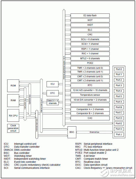
Figure 1. RX210 block diagram
RX210 Series Renesas Starter Kit
The Renesas Starter Kit for RX210 is intended as a user-friendly introductory and evaluation tool for the RX210 microcontroller. The board also provides a useful platform for evaluating the Renesas suite of development tools for coding and debugging, using High-performance Embedded Workshop as well As programming the device using E1 emulator and/or Flash Development Toolkit.
The Renesas Starter Kit for RX210 may be connected to the host PC using a simple RS232 serial connection or via the included USB E1 on chip debugging interface.
The purpose of the board is to enable the user to evaluate the capabilities of the device and its peripherals by giving the user a simple platform on which code can be run only minutes from opening box. It can also prove an invaluable tool in development by providing a useful test platform for code already debugged using one of our more powerful emulation tools.
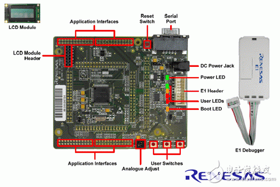
Figure 2. RX210 Series Starter Kit Outline Drawing
RX210 Series Renesas Starter Kit (RSK) Key Features:
This RSK provides an evaluation of the following features:
• Renesas yan programming
• User code debugging
• User circuitry such as switches, LEDs and a potentiometer
• Sample application
• Sample peripheral device initialisation code
The RSK board contains all the required solder processing for microcontroller operation.
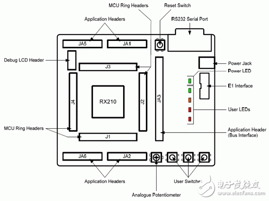
Figure 3. RX210 Series RSK Board Layout
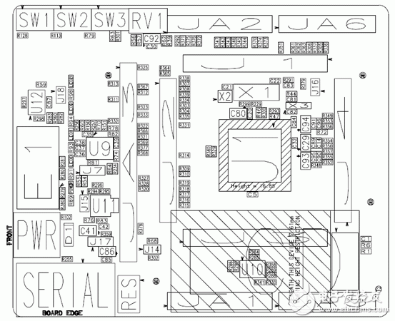
Figure 4. Top-level layout of RX210 Series RSK board
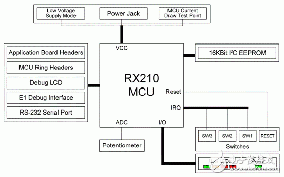
Figure 5. Block Diagram of RX210 Series RSK Board
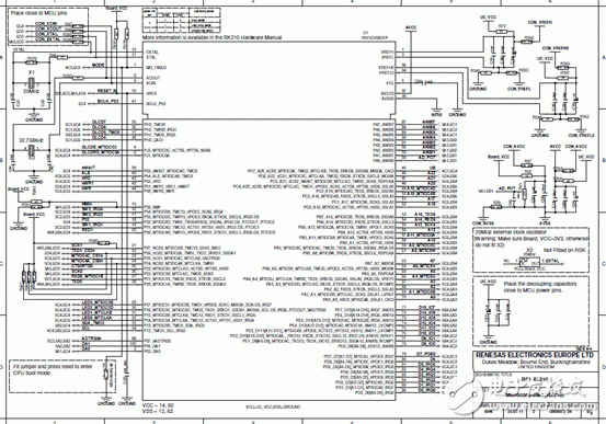
Figure 6. Circuit Diagram of RX210 Series RSK Board (1)
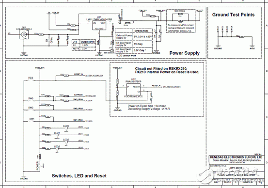
Figure 7. RX210 Series RSK Board Circuit Diagram (2)
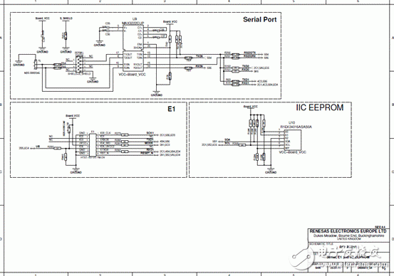
Figure 8. Circuit Diagram of RX210 Series RSK Board (3)
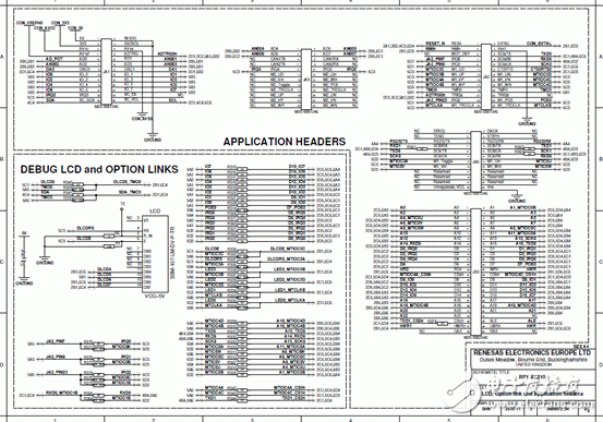
Figure 9. RX210 Series RSK Board Circuit Diagram (4)
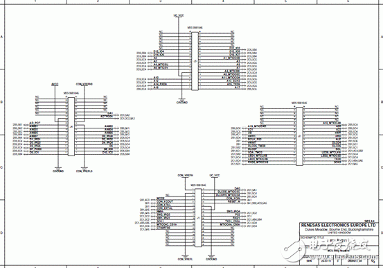
Figure 10. Circuit Diagram of RX210 Series RSK Board (5)
As soon as our company was established, the small size 4 wire resistive Touch Screen was first put into production,it range in size from about 2 inch to 22 inch,we provides a wide range of customization options to meet your requirements, including screen size, FPC outlet location, length, ITO glass thickness, LOGO and matte anti newton ring, bright surface treatment such as anti newton ring.we supply the best resistive touch screen,commercial touch screen,Glass touch screen, POS touch screen,GPS touch screen,Car touch screen,no drifting touch screen,stable touch screen,long life touch screen,high sensitive resistive touch screen,cheapest resistive touch screen.If you're interested 4 wire resistive touchscreen ,we are your best choice.
Our 4 wire resistive touch screen picture show:


Monitor Touch Screen Panel,4 Wire Touch Screen Panel,Resistive Touch Screen,Usb Controller Touch Screen,4 Wire Resistive Touchscreen,Best Touch Screen
ShenZhen GreenTouch Technology Co.,Ltd , https://www.bbstouch.com