As shown in Figure 2.7, the ideal clock model is a square wave with a 50% duty cycle and a fixed period. For one clock cycle, high pulse width, low pulse width, =+. Under normal circumstances, the internal logic of the FPGA device performs data input and output processing on the rising edge of each clock cycle. In the free time of the rising edges of two clocks, it can be used to perform a variety of complex operations. deal with. A time-consuming and complex computational process, which can often not be completed in one clock cycle, can be cut into several less time-consuming operations and then output the final result after several clock rising edges. The introduction of the clock signal not only makes all the digital operation processes "quantifiable", but also enables the synchronization of various unrelated operation processes to one beat.
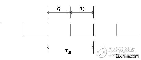
Figure 2.7 The ideal clock waveform
The clock source of FPGA device generally comes from the outside, we usually use the crystal oscillator (abbreviated as the crystal oscillator) to produce the clock signal. Of course, some of the larger FPGA devices will have dedicated clock management modules such as PLLs or DLLs that can multiply or divide clock signals. Because the clock signals used inside the FPGA device are often used not only for a single register, because in practical applications, hundreds of thousands of registers or more are likely to share a clock source, the delay from the clock source to different registers is also There may be large deviations (we often refer to clock network delays), and we know that this time difference is too large to be fatal. Therefore, FPGA devices have designed some routing pools called "global clock networks." With this dedicated clock network routing, the time difference of the same clock reaching different registers can be controlled to a very small range. And how can we ensure that the input clock signal can go "global clock network"? There are many ways for externally input clock signals, as long as the clock signal generated by the crystal is connected to the "global clock dedicated pin"; and for high fan-out control signals inside the FPGA, usually the tool software will automatically identify such signals The default connection to the "global clock network", and if designers do not worry, you can view the compiled report, and even manually add such signals. There are several basic issues to consider when designing and selecting a clock circuit:
â— What is the system clock frequency? (There may be more than one clock)
â— Is there an internal clock management unit available (usually there)? Its input frequency range (need to check the device manual for confirmation)?
â— Select dedicated clock input pins as much as possible.
With respect to the PCB layout design of the FPGA clock circuit, it is usually necessary to follow the following principles.
â— The clock oscillator source should be placed as close as possible to the dedicated pin of the FPGA clock to which it is connected.
â— Keep the clock line as straight as possible. If you cannot avoid cornering, use a 45-degree line and try to avoid T-shaped traces and right-angle traces.
â— It is not necessary to take the clock line at multiple signal layers at the same time.
â— Do not use vias for clock traces because vias can cause impedance changes and reflections.
â— Ground near the outer layer minimizes noise. If you use the inner clock line, you must have a good reference plane and walk the stripline.
â— The clock signal should have a termination matching circuit to minimize reflections.
â— Use point-to-point clock traces whenever possible.
â— As shown in Figure 2.8, the traces of the clock differential pair must be in strict accordance with the D>2S rule to minimize the crosstalk between adjacent differential pairs.
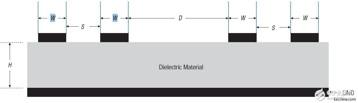
Figure 2.8 Clock Differential Pair Interval
â— Ensure that the entire differential pair has constant line spacing throughout the trace.
â— Ensure that the differential pair traces are the same length to minimize skew and phase shift.
â— Avoid using multiple vias during the same network trace to ensure impedance matching and lower inductance.
â— Keep high-frequency clock and USB differential signal pairs as short as possible.
â— Keep high-frequency clocks or periodic signals as far away as possible from high-speed differential pairs and any outgoing connectors (such as I/O connectors, control and data connectors, or power connectors).
â— Ensure that all traces have a continuous ground and power reference plane.
â— To minimize crosstalk, minimize the length of the high-frequency clock or periodic signal and high-speed signal and the length of the trace. The recommended minimum pitch is 3 times the clock signal and the nearest reference plane spacing.
â— When a clock drives multiple loads, use a low-impedance transmission line to ensure that the signal passes through the transmission line.
â— Use circuit vias for signal layer changes.
The delay of the synchronous clock should match the data. Ensure that the clock and the synchronous data bus are on the same layer to minimize the difference in transmission rates between different layers.
Uv Curing Film For Mobile Tablet
Uv Curing Film For Mobile Tablet,Tempered Glass For Mobile,Phone Curve Edge Protector,Local Tempered Glass
Shenzhen TUOLI Electronic Technology Co., Ltd. , https://www.hydrogelprotectors.com