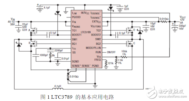
LTC3789 is a newly developed high-efficiency high-performance buck-boost switching regulator controller with input voltage from 4V to 38V. The output voltage can be higher than the input voltage. It can be lower than the input voltage of 0.8V~38V. Constant, up to 600KHz (200~600KHz). Works for current mode. The output current feedback loop provides support for battery charging, meeting a wide range of input and output 4V ~ 38V. With low noise in the work area, the LTC3789 is the ideal battery-powered system application IC for buck-boost.
The controller operating mode is determined by the MODE/PLLIN terminal. The MODE/PLLIN terminal can be selected between the pulse skip mode and the continuous operation mode. It allows the IC to synchronize to an external clock. The pulse skip type provides very low ripple at light loads. Same as in continuous working mode.
When the output voltage enters within 10% of the set value, the PG end gives an indicator, and the LTC3789 uses a 28 PIN 4mm & TImes; 5mm QFN package.
The LTC3789 requires four power MOSFETs externally. When VIN is turned off, VOUT is disconnected and the soft start time is adjustable. It is mainly used in automation systems and high-power battery power supply systems.
LTC3789 basic application circuit diagram, as shown in Figure 1.
The following describes the operation of the LTC3789, a highly efficient synchronous four-switch buck-boost controller.
Main loop controlThe LTC3789 is a current mode controller that provides an output voltage higher than, equal to or lower than the output voltage. LTC's proprietary topology and control architecture employ a current sense resistor. The voltage on the ITH pin is the output voltage of the error amplifier's EA, and the current on the inductor is controlled by the voltage on the ITH pin. The feedback voltage at the VFB pin is compared to the internal reference voltage of the error amplifier EA. If the input-output current regulation loop is implemented, the detection of the inductor current is controlled by detecting the feedback voltage or detecting the input-output current.
INTVCC/EXTVCC power supplyThe top and bottom MOSFET drivers and most of the internal circuitry are powered from the INTVCC. When the EXTVCC turns it on or is tied below 4.5V, an internal 5.5V low dropout regulator supplies the INTV to the VIN if EXTVCC rises. Above 4.8V, the 5.5V regulator is turned off, another LDO regulator INTVCC gives a stable voltage from EXTVCC, and the LTV of EXTVCC allows INTVCC to supply power from a more efficient external power supply, such as the output from the LTC3789, the maximum of EXTVCC The voltage is allowed to be 14V.
Internal charge pumpEach of the top MOSFET drivers draws charge from the floating boost capacitors CA and CB, which is typically charged by the INVTCC through an external diode when the MOS is turned off. When the LTC3789 only operates in the buck or boost interval, one of the top MOS is always on, an internal charge pump recharges the boost capacitor, and the boost diode has only a small leakage current, which keeps the MOS Turn on. Of course, if the diode leakage is large. The internal charge pump will not be able to charge the external boost capacitor sufficiently. An internal UVLO comparator always monitors the voltage across this capacitor and detects that the BOOST-SW voltage must not be lower than 3.6V, otherwise it will turn off the top MOSFET, approximately the clock. 1/12 of the cycle to allow the CA or CB to recharge.
Shutdown and startThe controller can be turned off by pulling the RUN terminal low to low level. When the RUN terminal voltage is lower than 0.5V, the LTC3789 enters the low quiescent current mode. Release the RUN terminal to allow the internal 1.2μA current source to charge it, pull the level up, and enable the controller again. When the RUN terminal is above the precision threshold of 1.22V, the internal LDO will supply power to the INTVCC. At the same time, a 6μA pull-up current will suddenly jump in and provide more hysteresis to the RUN terminal. The RUN terminal can also be pulled up externally or directly by a logic circuit. Be careful not to exceed the absolute maximum voltage of this terminal by 6V.
The start of the controller output voltage VOUT is controlled by the voltage on the SS terminal when the SS terminal voltage is lower than the internal reference voltage of 0.8V. The LTC3789 regulates the VFB voltage by replacing the 0.8V reference with the voltage on the SS. This allows the SS terminal to use an external capacitor to regulate the soft start. This capacitor is connected to the SS terminal to GND. An internal 3μA pull-up current charges this capacitor, creating a voltage ramp on the SS side. As the voltage at the SS terminal rises linearly, from 0V to 0.8V, the output voltage VOUT also rises from 0V to the set voltage value synchronously. In other words, the SS terminal can be used to determine the output trajectory of the output voltage VOUT following another power supply. The controller can be disabled when RUN is pulled low. When INTVCC is lower than the undervoltage lockout value of 3.4V, the SS terminal is pulled low by the internal MOSFET to enter the undervoltage lockout state, the controller is disabled, and the external power MOS is in the off state.
Power switch control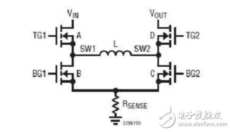
The figure above shows a simplified block diagram of how four switches are connected to the inductor, VIN, VOUT and GND.
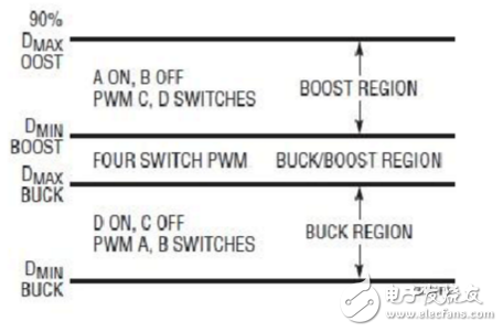
The figure above shows the operating area of ​​the LTC3789 duty cycle D function. The power switch tube is properly controlled for continuous zone switching.
Boost area (VIN "VOUT")In the boost region, the switch A is always on, and the synchronous switch B is always off. In each cycle, the switch C is first turned on, and when the synchronous switch C is turned on, the current on the inductor is detected. When the peak current on the inductor detects a demand exceeding the reference voltage and is proportional to the voltage on the ITH pin, the switch C is turned off while the switch D is open for the remainder of the cycle. Switch C and Switch D alternately open, like a typical synchronous boost regulator. The duty cycle of switch C is reduced until the minimum duty cycle of the converter reaches DMIN_BOOST, as follows:

Switch D is always in the on state, and switch C is always in the off state. At the start of each cycle, the synchronous switch B is first turned on, and the inductor current is detected when the synchronous switch B is turned on. When the detected voltage falls below the reference voltage, it is proportional to VITH, and the synchronous switch B is turned off, and the switch A is turned off. Turn on and keep the entire cycle, then switch A and B alternate. As with the typical BUCK circuit, the duty cycle of switch A increases until the maximum duty cycle DMAX allowed, given by:

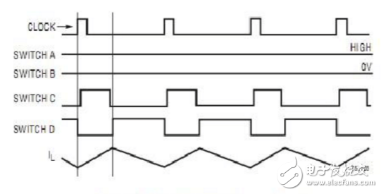
When VIN approaches VOUT, the controller enters the BUCK-BOOST region. Figure 4 shows a typical waveform in this region. At the beginning of the clock cycle, if the controller starts with B and D, the controller first operates in the BUCK region. When ICMP is activated, switch B is turned off and switch A is turned on at 120. At the clock phase, switch C is turned on, and LTC3789 starts working for BOOST until ICMP is activated. Then, switch D is turned on for the remaining clock cycle. If the controller turns on switches A and C, it first operates in the BOOST state until ICMP touch switch D is turned on, at 120. Switch B is also turned on, causing it to operate in the BUCK state. Then, ICMP is activated, switch B is turned off, and switch A is turned on until the end of the cycle.
The figure below shows a typical waveform for the boost region. If VIN is close to the output voltage, it will enter the buck-boost region.

AC Input : 100V to 240V, DC Output: 12 volt at 2 amp rating . Please refer to the ASIN :B0746GCGQ8 if u need 10 units.
Type : Regulated Switching Power Supply with 2.1mm x 5.5mm plug , center positiveManufactured with high quality material and built-in protection of over current, over voltage, short circuits .
COMPACT DESIGN and LOW CONSUMPTION makes it ideal for taking around and using at home.
12v wall charger,12v switching adapter,(12V/2A) Switching Mode Power Adapter Wall Charger,12V 2A Power Supply Adapter,12 Volt 2 Amp Power Adapter,12V 3A Power Supply Adapter,12v3a wall charger
Shenzhen Waweis Technology Co., Ltd. , https://www.szwaweischarger.com