About the author: Zhang Falin, has been engaged in the research and development of embedded system software and hardware for more than 20 years, and currently works as the chief electronic engineer of Shanghai Future Partner Robot Co., Ltd. In-depth understanding of the difficulties and pain points in various links from product demand analysis, program demonstration design, technology research and development, productization, testing and certification, mass production, etc., solved a large number of R&D, productization and production problems, participated in or led the development of many industries Automation equipment, communication equipment, monitoring systems, Internet of Things and robotics products have all been put into mass production and sales.

A newly designed circuit board becomes PCBA after SMT, wave soldering or manual soldering, which is the first step in the long march. However, from PCBA to final finalization and delivery to the factory for mass production, a series of tests and verifications are required in the middle. Many young electronic engineers are not clear about PCBA and electronic product system debugging steps and specific requirements at each stage, which often leads to inefficient development and debugging, and even damages the circuit board to be tested. What is even more frightening is that the design with functional or performance defects is transferred to the mass production stage, causing huge losses to the company. Based on years of personal practice, the author summed up the nine steps from PCBA to product finalization, and efficiently completed the research and development of a variety of electronic products.
The first step visual inspection
The PCBA that has just been mounted and delivered to the electronic engineer is shown in Figure 1. Experienced engineers can quickly find many design, material and process problems through visual inspection, which can save a lot of follow-up debugging time.
1.1. Carefully compare the circuit diagram, check whether the version of the schematic diagram, PCB diagram, and BOM are consistent with the actual product you get, and whether the important components actually welded by the PCBA are consistent with the circuit diagram.
1.2 Check whether there are tin beads and dross on the board, continuous welding, and whether there are obvious missing parts and missing welding; gently pull out relatively large components, especially electrolytic capacitors, high-power inductors and hand plugs, carefully Observe whether the reconnecting position is centered accurately and whether the solder joints are firm.
1.3 Pay attention to check the power line arrangement, important IC mounting direction, diode AK direction, polarity of polar capacitor, and the notch direction of the connector.
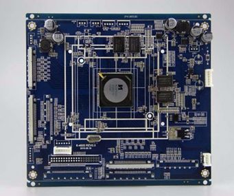
Figure 1 PCBA physical map
Second step impedance test
This step is relatively simple, but extremely important. Many serious problems are caused by ignoring this step. Please be sure to repeatedly verify the polarity and voltage of the power supply that needs to be loaded. Use a multimeter to check whether there is a short circuit between each input and output power supply and the ground, and whether there is obvious impedance abnormality. If there is any abnormality, it must be ruled out. lucky.
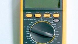
Figure 2 Digital Multimeter
The third step of power-on inspection
With anxious mood, I guess you can't wait to power up your circuit board. Well, you can power up, but you must be prepared to make a heroic sacrifice at any time to power up correctly. Connect the negative pole of the power cord to the negative pole of the experimental power supply. After confirming that the output voltage of the experimental power supply is correct, gently lap the positive pole of the power cord to the positive pole of the experimental power supply terminal. Don't rush to observe the waveform and data with the instrument. Only care about the moment the PCBA is powered on. Whether there are abnormal phenomena, such as smoke, fire, electric spark, abnormal smell, device burst, etc. The specific tragic symptoms are shown in Figure 3. If there is an abnormality, remove the power cord immediately, return to the first step to troubleshoot the problem, and perform this step again after the problem is found and resolved. After confirming that there is no abnormality, the power can be officially turned on. After observing for a period of time, no abnormality or obvious hot IC can be entered to the next step.
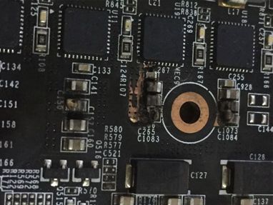
Figure 3 Smoking circuit board
The fourth step static test
After the PCBA is officially powered on, follow the steps below to perform a static test according to the hardware design specification.
4.1 Working voltage and working current measurement
The test of DC voltage is very convenient and can be measured directly. The measurement of current is not very convenient, and two methods are usually used to measure it. If the circuit has test points on the printed circuit board, it can be connected in series with an ammeter to directly measure the current value, and then connect it with solder. If there is no test hole, the DC voltage can be measured, and then the DC current can be calculated according to the resistance value. For circuits with multiple power supplies, the power-on sequence of each power supply must be tested, as shown in Figure 4.
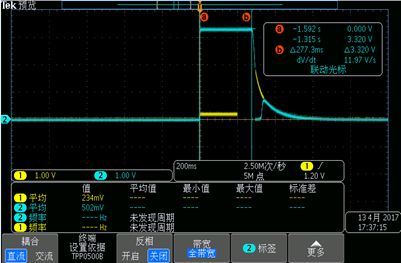
Figure 4 Power-on sequence diagram
4.2 Processor minimum system default state test
Need to confirm the polarity and waveform of the processor reset level, the frequency of the crystal oscillator circuit, the state of the input configuration pin, and the initial state of the output control pin. The waveform diagram of the single-chip crystal oscillator circuit is shown in Figure 5.
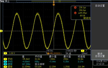
Figure 5 Waveform diagram of single-chip crystal oscillator circuit
4.3 Initial state test of logic circuit
Focus on whether the chip select signal, enable signal and the default state of the configuration pins meet the requirements. The default state of the DIR_485 pin as shown in Figure 6 is low.
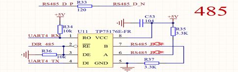
Figure 6 RS-485 bus drive circuit diagram
4.4 Analog circuit operating point test
Need to test and optimize the DC static operating points of amplifiers, transistors, MOS tubes, etc. As shown in Figure 7, the resistance values ​​of R1 and R2 need to be calculated according to the parameters of the MOS tube and adjusted according to the measured results.
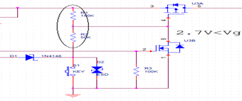
Figure 7: Schematic diagram of MOS tube operating point debugging
Fifth step function debugging
This stage usually requires software driver cooperation, and various professional instruments and equipment such as signal generators, logic analyzers, oscilloscopes, spectrum analyzers, electronic analog loads, etc. are needed.
5.1 Open up the processor debugging interface to realize software program download operation and status output; as shown in Figure 8.
Figure 8 Schematic diagram of Jtag emulator debugging
5.2 Verify the human-computer interaction function, and the information indication function is normal;
5.3 Through program control, drive the digital circuit to observe whether the output signal waveform, amplitude, pulse width, phase and dynamic logic relationship meet the requirements. Verify logic control and communication interface functions, the input status is correct and the output status is controllable;
5.4 Adjust the AC path components of the analog circuit, such as capacitors, inductances, etc., so that the waveform, amplitude, frequency and other parameters of the AC signal meet the design requirements;
5.5 Input a single step signal to test whether the logical relationship of the circuit state change meets the requirements;
5.6 Verify that the drive circuit works normally under no-load or light-load conditions.
5.7 After all the function debugging is completed, the function debugging report should be submitted as shown in Table 1.
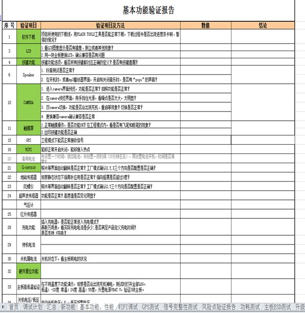
Table 1 Function debugging and verification report
The sixth step performance test
After the circuit is dynamically debugged, the required technical indicators can be measured. Such as the transmission speed, bit error rate, wireless transmission distance, signal-to-noise ratio, etc., test and record the test data, analyze the test data, and finally make a test conclusion to determine whether the technical indicators of the circuit meet the design requirements. If there is any discrepancy, you should carefully check the problem, usually to adjust and change some component parameters or software configuration. If it still fails to meet the requirements, some part of the circuit or configuration should be modified, or even the entire circuit should be revised again. Therefore, it is required to be serious and meticulous in the whole process of design, and to consider issues more thoroughly. The specific test results are shown in Table 2.
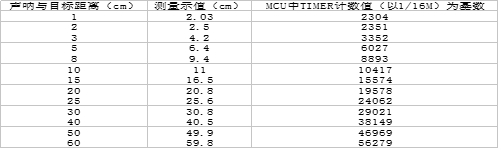
Table 2 Performance Test Analysis Table
Seventh step conformance test
After performance testing and confirming that the design requirements are met, at least 3 or more functional and performance consistency evaluations are required according to the actual situation, and comparison tests for voltage, current, delay, signal waveforms, etc., if there are obvious deviations, you must not take it lightly. It is necessary to carefully analyze possible deficiencies in design, materials, processing technology, or debugging and testing programs. As shown in Table 3, it can be analyzed whether there is an accidental problem or a batch problem.
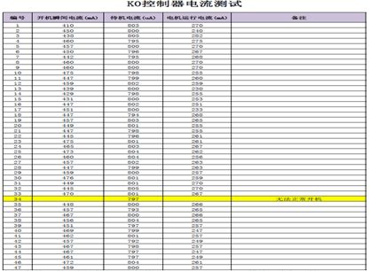
Table 3 47 sets of product working current consistency test
The eighth step system joint debugging
The PCBA that has passed the conformance test needs to be installed and fixed in the whole system for system joint debugging. In principle, the system-level conformance test must also be carried out.
The most common problem in the process of system joint debugging is the interference between PCBA and structure; the influence of wireless communication antenna position on communication performance; the performance degradation caused by the deterioration of heat dissipation conditions, the function or performance degradation caused by the communication error rate, and the audio and video parts are affected. The influence of the cabinet; motor stall or overheat protection caused by insufficient load capacity, various abnormalities caused by insufficient system power supply capacity, etc. Due to the wide variety of electronic products, it is necessary to conduct a careful investigation in conjunction with the system block diagram. The system block diagram of a product is shown in Figure 9.
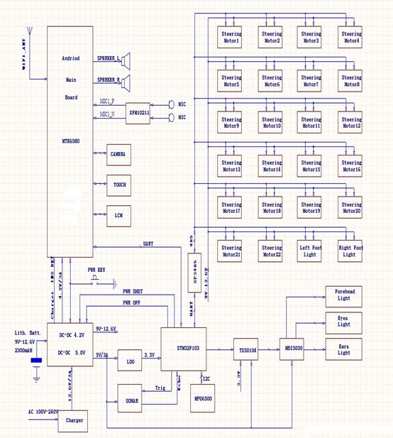
Figure 9 System block diagram of a product
Ninth step type test
Type testing is an important link in the R&D phase of electronic products, a key node in the transition from R&D to production, and an important basis for product failure. The specific test content and requirements vary according to the type and requirements of the product. However, the general scope is not much different from the test items. For example, the type test outline of a product is shown in Figure 10.
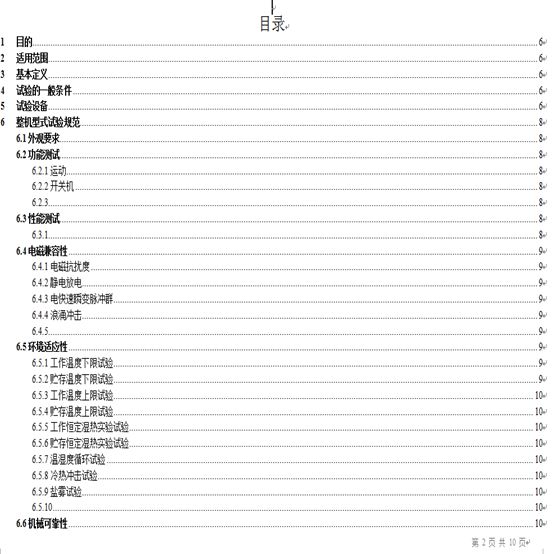
Figure 10 A product type finalization test outline
Concluding remarks
Current electronic products are all-encompassing, and integrated chips and functional circuits are also emerging in an endless stream. Coupled with the high correlation of embedded system machinery, electronics and software, the difficulty of PCBA to system joint debugging is gradually increasing. In addition, due to the fierce market competition and the continuous compression of the electronic product development cycle, this places higher requirements on the debugging capabilities and capabilities of the electronic engineer from PCBA to product finalization. Although the form of electronic products and the specific application of electronic technology are different, the basic process, steps and precautions of debugging are highly connected. The nine-step debugging method has a certain reference and reference effect for electronic engineers in various industries.
Adjustable Aluminum Laptop Stand,Laptop Stand Aluminium Adjustable Portable,Aluminum Laptop Stand Adjustable Height,etc.
Shenzhen Chengrong Technology Co.ltd is a high-quality enterprise specializing in metal stamping and CNC production for 12 years. The company mainly aims at the R&D, production and sales of Notebook Laptop Stands and Mobile Phone Stands. From the mold design and processing to machining and product surface oxidation, spraying treatment etc ,integration can fully meet the various processing needs of customers. Have a complete and scientific quality management system, strength and product quality are recognized and trusted by the industry, to meet changing economic and social needs.

Adjustable Aluminum Laptop Stand,Laptop Stand Aluminium Adjustable Portable,Aluminum Laptop Stand Adjustable Height
Shenzhen ChengRong Technology Co.,Ltd. , https://www.dglaptopstandsupplier.com