1, collector open circuit output principle
Open Drain and Open Collector are often encountered in circuits. The "drain" mentioned in the open-drain circuit concept refers to the drain of the MOSFET. Similarly, the "set" in the open collector circuit refers to the collector of the triode. In digital circuits, they are referred to as OD gates and OC gates, respectively.
The open collector circuit is a sink current output device. In the off state, the open collector output is connected to ground; in the on state, the open collector output is left floating. Therefore, the open collector output requires a source current input interface. A schematic diagram of a simple open collector output circuit is shown in the table below.
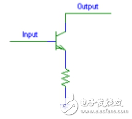
A typical open collector circuit is shown below. The collector of the triode on the right side of the circuit is connected, so it is called open collector, and the triode on the left is used for inverting action. When the left input is "0", the left triode is turned off, and VCC is applied to the right triode through the resistor. Base, the right triode is turned on, the right output is connected to ground, and the output is "0".
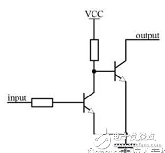
It can be seen from the circuit in the figure that the open collector cannot output a high level. If you want to output a high level, you can add a pull-up resistor to the output. Therefore, the open collector output can be used for level shifting, and the pull-up resistor is pulled up to a different voltage to achieve different level shifting.
Used as a drive. Since the collector of the output tube of the OC gate circuit is suspended, an external pull-up resistor Rp needs to be externally connected to the power supply VCC. The OC gate uses a pull-up resistor to output a high level. In addition, in order to increase the driving capability of the output pin, the selection principle of the pull-up resistor value should be large enough to reduce the power consumption and the current sinking capability of the chip; The drive current considerations should be small enough.
When the OC gate outputs are connected together, the "wire-to-logic" logic relationship can be realized by connecting a resistor to the external power source. As long as the resistance value of the resistor and the value of the external power supply voltage are properly selected, it can ensure that the high and low levels of the output meet the requirements, and the load current of the output triode is not too large.
In addition to the multi-gate line and logic relationship, the open collector output can also be used to directly drive large current loads such as relays, pulse transformers, and indicator lights by using high-power transistors.
2. Application of open collector output
Application one:
Realize NAND or Logic, use level shifting, and use it as a driver. Since the collector of the output tube of the OC gate circuit is suspended, an external pull-up resistor Rp needs to be externally connected to the power supply VCC. The OC gate uses a pull-up resistor to output a high level. In addition, in order to increase the driving capability of the output pin, the selection principle of the pull-up resistor value should be large enough to reduce the power consumption and the current sinking capability of the chip; The drive current considerations should be small enough.
Application 2:
The logical function of "AND" can be realized by the line and logic, that is, the direct interconnection of two outputs (including two or more). In practical applications such as bus transmission, the output terminals of multiple gates need to be connected in parallel, and the general TTL gate outputs cannot be directly connected in parallel. Otherwise, the output tubes of these gates form a large short-circuit current due to low impedance. Current), which burns out the device. In hardware, it can be implemented with an OC gate or a three-state gate (ST gate). To achieve line and OC gates, a pull-up resistor should be added to the output port.
Application three:
The tri-state gate (TS gate) is mainly used in multiple gate output shared data buses. To avoid multiple gate outputs occupying the data bus at the same time, only one of the gate enable signals (EN) is allowed to be active ( If the output of the tri-state gate is a push-pull low-impedance output and does not need to be connected to a pull-up (load) resistor, the switching speed is faster than the OC gate, and a tri-state gate is often used as an output buffer.
Second, open drain output1, open drain output principle
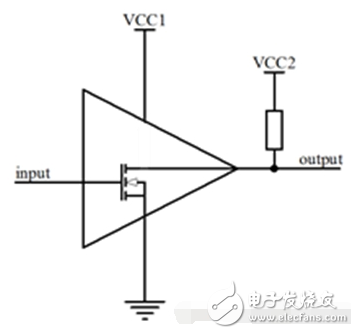
As with the open collector, as the name implies, an open drain circuit is a circuit that outputs from the drain of a MOSFET. A typical use is to add a pull-up resistor to the power supply on the circuit outside the drain as shown. The complete open drain circuit should consist of an open-drain device and an open-drain pull-up resistor. The value of the pull-up resistor R here determines the speed of the rising/falling edge of the logic level shift. The larger the resistance, the lower the speed and the lower the power consumption. Therefore, when selecting a pull-up resistor, both power consumption and speed should be considered. Standard open drain feet generally have only the ability to output. Add other judgment circuits to have the ability to input and output in both directions.
The I/O of many microcontrollers and other devices is open-drain, or can be configured as an open-drain output. For example, the P0 port of the 51 MCU is an open-drain output. In practical applications, multiple open-drain output pins can be connected to a single line, thus forming a "line-to-logic" relationship. Note that this common point must be connected to a pull-up resistor. When any of these pins goes to logic 0, the logic on the open drain line is zero. This method is used to judge the bus occupancy status in an interface bus such as I2C.
Like the open collector, the drive capability of the external circuit is used to reduce the drive inside the IC. When the internal MOSFET of the IC is turned on, the drive current flows from the external VCC through the pull-up resistor and then through the MOSFET to GND. The IC requires only a very low gate drive current, so open drain is also commonly used in drive circuits.
2, characteristics
1) Reduce the drive inside the ic by using the drive capability of the external circuit. Or drive a load that is higher than the chip supply voltage.
2) It is possible to connect multiple open-drain pins to one line. Through a pull-up resistor, a "logical" relationship is formed without adding any devices. This is also the principle that i2c, smbus and other buses determine the bus occupancy status. If the totem output is connected, a pull-up resistor must be connected. When the capacitive load is connected, the falling edge is the transistor inside the chip, which is an active drive, and the speed is fast; the rising delay is a passive external resistor, and the speed is slow. If the speed requirement is high, the power consumption will be large. Therefore, the choice of load resistor must balance power consumption and speed.
3) The transfer level can be changed by changing the voltage of the pull-up power supply. For example, a pull-up resistor can be used to provide a ttl/cmos level output.
4) The open-drain pin is not connected to an external pull-up resistor, and only outputs a low level. In general, open drain is used to connect different levels of devices for matching levels.
5) The normal CMOS output stage is the upper and lower tubes. The removal of the upper tube is open-drain. The main purpose of this output is two: level shifting and line sum.
6) Because the drain is open, the post-stage circuit must be connected to a pull-up resistor, and the power supply voltage of the pull-up resistor can determine the output level. This way you can convert at any level.
7) Line and function are mainly used when there are multiple circuits to pull down the same signal. If the circuit does not want to pull low, it will output high level, because the tube above open-drain is removed, the high level is It is realized by an external pull-up resistor. (And the normal CMOS output stage, if one output is high and the other is low, it is equal to the power supply short circuit.)
8) open-drain provides a flexible output mode, but it also has its weakness, which is the delay of the rising edge. Because the rising edge charges the load through an external pull-up passive resistor, when the resistance is selected, the hour delay is small, but the power consumption is large; otherwise, the delay is large and the power consumption is small. Therefore, if there is a requirement for the delay, it is recommended to use the falling edge output.
3. What is line or logic and line and logic?
Connect a pull-up resistor to the power supply vcc or vdd and the collector c or drain d of n npn or nmos transistors on a node (line). The emitter e or source s of these transistors are connected to the ground. On, as long as one transistor is saturated, this node (line) is pulled to the ground level.
Because the bases of these transistors inject current (npn) or gate plus high (nmos), the transistors are saturated, so the relationship of these bases or gates to this node (line) is NAND or non-nor logic. If an inverter is added after this node, it is OR logic.
Note: Personal understanding: line and, pull up the resistor to the power supply. (~a)&(~b)=~(a+b), it is easier to understand the origin of the line and the concept by the formula;
If you use a pull-down resistor and a pnp or pmos tube, you can construct a non-nand logic, or a negative logic relationship and/or logic.
Note: Wire or connect the pull-down resistor to ground. (~a)+(~b)=~(ab);
These transistors are often collector open oc or source open od outputs of some logic circuits. This logic is usually called line and / line or logic. When you see the oc or od outputs of some chips connected together, and there is a pull-up resistor, this is the line or / line, but sometimes pull up The resistor is placed in the input of the chip.
By the way, if the output of the oc or od chip is not connectable, the bidirectional outputs on the bus bus are managed together, and only one output can be used, while the other is high impedance. enter.
KNL6,KNL8 Residual Current Circuit Breaker
KNL6,KNL8 Moulded Case Circuit Breaker is MCCB , How to select good Molded Case Circuit Breaker suppliers? Korlen electric is your first choice. All moulded Case Circuit Breakers pass the CE.CB.SEMKO.SIRIM etc. Certificates.
Moulded Case Circuit Breaker /MCCB can be used to distribute electric power and protect power equipment against overload and short-current, and can change the circuit and start motor infrequently. The application of Moulded Case Circuit Breaker /MCCB is industrial.
Korlen electric also provide Miniature Circuit Breaker /MCB. Residual Current Circuit Breaker /RCCB. RCBO. Led light and so on .
KNL6,KNL8 Molded Case Circuit Breaker,Small Size Molded Case Circuit Breaker,Electrical Molded Case Circuit Breaker,Automatic Molded Case Circuit Breaker
Wenzhou Korlen Electric Appliances Co., Ltd. , https://www.zjmoldedcasecircuitbreaker.com