Keywords : test system switch construction
This article refers to the address: http://
Test systems often measure large amounts of signals with a small number of instruments. This design approach limits costs and limits test throughput. Conversely, if the system has all the signals tested and enough instruments, although the throughput can be increased faster, it is usually costly and uneconomical.
The traditional approach to low-cost test systems is to switch a digital voltmeter (DVM) between several signals. If only two signals are included, the DVM is connected to a single pole double throw switch (SPDT), which is connected to one of its two signals by a single pole. A double pole double throw (DPDT) configuration is suitable if the high and low ends of the switching signal must be switched. For 4 signals, a double pole 4 throw (DP4T) switch is available.
There are also more than 2 knives in the application. For example, a 4PDT (4-pole double throw) switch can support 4-wire or kelvin connection ohms measurements on two components. A 6PDT switch provides drive protection and 4-wire ohms measurements. Of course, such switching terms can be extended indefinitely.
The multiplexer is described from a similar knife and throw concept, expressed as n x m, where n is the number of knives and m is the number of throws. Some vendors represent a single-pole 8-way multiplexer as 1×8, while others call it 8×1. In the multiplexer, all the knives are usually connected together. For example, a 2x8 multiplexer can be used to turn on one of eight differential signals to a differential voltmeter.
The same n x m is used to describe the switch matrix, but in an actual matrix, any of the n rows can be connected to any of the m columns. For example, a 2×8 matrix can be connected to any row or two rows at the same time to any column of the column. If you want this matrix to be used as a differential multiplexer, it will be deteriorated and costly due to the large number of switches.
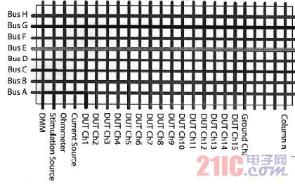
Typically a switch matrix is ​​used to turn on multiple instruments in a multiple input channel. Figure 1 shows the column-based matrix switching instrument, source, and DUT (channel 1), and the DMM measures the voltage. At the same time, unused inputs are grounded. In this configuration, the matrix rows act like a set of columns to which the buses are connected together.

In the row-based configuration, the test instrument and source are configured in different rows, and the columns are specifically configured with DUTs. You can choose any combination of rows and columns. It is important to program the switch correctly to prevent short circuits. In some cases, a blocking matrix can be used to avoid the cost of the matrix. These matrices allow only one row to be connected to a particular column. Depending on the switching flexibility required, a few multiplexers can be combined to form a sparse matrix that supports only a subset of all possible row-column combinations.
The row and column turn-on sequence is also important. Usually, the first open and close switch is used to ensure that the instantaneous short circuit does not occur between incompatible signals. When developing a test program, the switch configuration software can monitor the programmed instrument and disable switch changes when the connection is broken. The responsibility of the test programmer is the application of the matrix to make the test system and the DUT secure.
RF test example
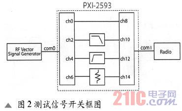
A simplified test system for RF radio IF (intermediate frequency) rejection measurements is shown in Figure 2. Both the FM signal power and the carrier frequency are controlled. Measure the radio audio output across a 4 ohm load (analog speaker). A measuring instrument (not shown) is directly connected to the radio input and output.

Both the RF signal and the radio are tuned to 90.1 MHz. In the first part of the test, the -3dB limit sensitivity measurement, the RF power is reduced from the reference level to the audio output down to 3dB. The radio IF rejection is then calculated using the RF power level.
Second, the signal carrier frequency drops to 10.7 MHz, but the radio remains tuned to 90.1 MHz. Monitors the increase in radio output level as the RF signal power level increases.
Multiplexer
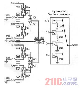
National Instruments' PXI-2593 switch module can be used in unterminated configurations such as four 3x1, dual 8x1 or single 16 or 17x1 multiplexers. Add a dual 4x1 or single 8x1 termination multiplexer for external 50 ohm terminations to support high frequency signals above 500 MHz. A detailed illustration of this configuration is shown in Figure 3.

In general, the complete switching module characterization parameters are isolation, return loss, and insertion loss. In practice, the use of a vector network analyzer to measure the performance of a module or individual relays can quickly provide complete S-parameter information. The amount of isolation and loss can be derived from the S parameter.
There is often a certain simplification. For example, a relay that is physically identical from the input or output will be equal or very close from output to input transmission S12 and from input to output transmission S21.
In the radio test set, the 500MHz switching performance index greatly exceeds the highest signal frequency of 90.1MHz. However, for RF applications, the switching performance of the bandwidth is critical. For example, how well the switch matches the 50 ohm characteristic impedance of the test system? A bad match is equivalent to a large voltage standing wave ratio (VSWR), which results in a test signal that is reflected and distorted by the pattern.
The VSWR (DC to 200MHz) of the PXI-2593 is guaranteed to be less than 1.4:1. Its typical performance plot shows that the VSWR is only greater than 1.1:1. VSWR=(1+|Г|)/(1-|Г|), where 1Г1 is the reflection coefficient value. For these VSWR limits, the corresponding input reflection coefficient ranges from 0.167 to 0.048, or about 17% to 5%.
The return loss is often indicated instead of the reflection coefficient. Return loss = -20log (| Г|), for the wireless test example, it is 15.5dB ~ 26.4dB. The larger the value, the greater the ratio of power to reflected power through the switch. In other words, a larger return loss value means that more input power is present at the output.
Consider insertion loss in the same VSWR range. If the signal power is lost by 16.7% due to reflection at the input, 83.3% of the signal power reaches the output. The 0.833:1 ratio is the basis for the insertion loss calculation. Insertion loss = 10 log (output / input). Corresponding to 1.4:1 and 1.1:1 VSWR insertion loss is 0.8dB and 0.2dB, respectively. A typical performance plot shows an insertion loss of 0.2 dB at 100 MHz.
isolation
When the switch is turned on and the signal path is completely cut, a small portion of the signal is still coupled to the output. Isolation describes the portion of the input signal that is coupled to the output. As the frequency increases, the switch isolation decreases because of the capacitance at the break contact. However, different relays have low enough capacitance to support switching to 1 GHz or 2 GHz signals, even up to 40 GHz.
For example, the highest density switch module uses a small reed relay as the switch element. In addition to the small features, the reed relay has the characteristics of very good reliability, low cost and wide index range. Since the two reeds are close to each other in the glass tube, the minimum capacitance of the switch opening is approximately 0.2 pF.
There is a BGA packaged relay that is a leadless device specifically designed to match a 50 ohm transmission line. The input and output signal paths of the BGA relay are designed as RF transmission lines with an RF impedance of nearly 50 ohms throughout the relay. Although this relay has a 11.5 GHz, -3 dB bandwidth, its isolation is only 10 dB at 5 GHz. Although this relay has good matching characteristics, it produces good return loss (35dB at 1GHz and 20dB at 5GHz), but when the relay is turned on, 10% of the input signal leaks to the output (at 5GHz).
The capacitive coupling model used to discuss isolation consists of a voltage source on one open junction, a stray capacitance across the junction, and a 50 ohm load from the other junction to ground. Based on this non-simplified model, the 0.28pF capacitor corresponds to 10dB isolation (at 5GHz) or 41dB isolation (100MHz).
The isolation of the PXI-2593 multiplexer is not specified, but is typically at 100MHz with isolation greater than 90dB. The type of relay indicated in the performance indicator is an electromechanical latching relay. This high-frequency electromechanical relay (such as G6Y) provides at least 65dB isolation at 900MHz. Although the PXI-2593 multiplexer does not use a reed relay, it is possible to achieve very high isolation at high frequencies. A T-shaped configuration in which two relays are connected in series with the third relay, from the intermediate point to the parallel capacitive coupling signal to ground. This method requires 3 relays, and the two relays in series are mismatched, which will deteriorate the overall insertion loss.
In order to achieve good loss and isolation utilization time at very high frequencies to determine the coherent sampling frequency. Review the same 8-bit graph again and divide the data into two segments (Figure 2). Due to the segmentation, the data samples are no longer arranged in the normal chronological order, but are interleaved, so the sampled waveforms are reordered after the acquisition is complete. The sampling rate of CIS is given by:
SR=KN/Tb(NL+K)
The factor K is variable and maintains a sampling rate of 10 MS/s for any length and rate.
Near real-time sampling
The NRO uses CIS technology, and the sampler is locked to the clock recovered from the input signal. The sampling rate is slightly lower than 10MS/s, so the sampling rate is not a strict fractional multiple of the data rate, so the sampling is repeated at the same point in the graph. get on. The oscilloscope continuously captures data and has a data memory length of 4M points up to 512M points.
The above analysis shows that NRO does not collect data sequentially, and it is necessary to reorder the recorded data and reconstruct the waveform. Due to differences in data acquisition techniques, the CIS method collects data at least 50 times faster than sequential sampling techniques (10MS/S for 200KS/S); data points are 1000 times more (4M points versus 4K points). The effective bandwidth of the NRO is between 20 GHz and 100 MHz.
NRO is often used to capture duplicate data patterns. However, eye diagram testing and jitter measurements can also be performed on non-repeating signals, including serial serial data streams. The sampling pulse of the CIS time base is phase-locked with the clock signal. The RMS jitter of the CIS time base is generally less than 600 fs, and the optional high stability time base can provide RMS jitter of less than 200 fs. In CIS mode, the 4M point basic storage length can be used to decompose the jitter component on the long serial data pattern; when the storage length is extended to 512M point, it can capture, display and measure nearly millions of bits of code.
Spring Terminal Block,Spring Clamp Terminal Block,Spring Loaded Terminal Blocks,Spring Terminal Connector
Cixi Zhongyi Electronics Factory , https://www.zypcbboards.com