Electromagnetic compatibility (EMC) refers to the ability of a device or system to operate in its electromagnetic environment and to produce unacceptable electromagnetic interference to any device in its environment. Therefore, EMC includes two requirements: on the one hand, the electromagnetic interference generated by the equipment in the normal operation process cannot exceed a certain limit; on the other hand, the appliance has certain electromagnetic interference in the environment. The degree of immunity, ie electromagnetic sensitivity.
The main research object of electromagnetic compatibility1 Various artificial noises, such as transmission line corona noise, car noise, contactor's own noise and noise caused by discharge when the conductor is turned on, electrical locomotive noise, urban noise, etc.
2 The impact of various utility equipment (transmission lines, communications, railways, highways, petroleum metal pipelines, etc.) in the shared corridor.
3 Reflection problems caused by large buildings such as super high-rise buildings, power lines, and iron towers.
4 The role of the electromagnetic environment in humans and various living things. These include power frequency fields such as strong wires, medium and short waves, and the effects of microwave electromagnetic radiation.
The effect of 5 nuclear electromagnetic pulses. Electromagnetic pulses generated by high-altitude nuclear explosions can destroy command, control, communications, computer and reporting systems on the ground.
6 SPECTEST technology. Its substance is a series of research work on information reception and protection from electromagnetic radiation and information leakage of information equipment.
7 Electronic device malfunction. In order to prevent malfunction, measures must be taken to improve the anti-interference ability of the equipment.
8 spectrum allocation and management. The radio spectrum is a limited resource, but it is not consumable. It must be managed scientifically and fully utilized.
9 electromagnetic compatibility and measurement.
10 natural influences, etc.
1 Use a perfect shield to prevent external radiation from entering the system, and to prevent the interference energy of the system from radiating outward. The shield should be kept in good condition, and the necessary doors, joints, vents and cable holes should be properly handled, and the shield should be reliably grounded.
2 Design a reasonable grounding system, the small signal, large signal and the circuit that generates the interference should be grounded as far as possible, and the grounding resistance should be as small as possible.
3 Using appropriate filtering techniques, the passband of the filter is properly selected to minimize leakage losses.
4 Using the limiting technique, the clipping level should be higher than the working level and should be limited in both directions.
5 Correctly select the connecting cable and wiring method, and replace the long cable with optical cable if necessary.
6 using balanced differential circuit, shaping circuit, integration circuit and gating circuit technology,
7 system frequency allocation should be appropriate. When there are multiple main frequency signals working in a system, try to avoid the frequency of each signal and even avoid the resonant frequency of the other party.
8 All kinds of equipment in the shared corridor should maintain a large gauge when conditions permit, so as to reduce the mutual influence.
Basic principles of electromagnetic compatibility design
GroundingGrounding is a very important issue for electronic devices. There are three grounding purposes:
(1) Grounding enables all unit circuits in the entire circuit system to have a common reference zero potential, ensuring that the circuit system can operate stably.
(2) Prevent interference from external electromagnetic fields. The grounding of the casing can cause a large amount of electric charge accumulated on the casing due to electrostatic induction to be discharged through the earth, otherwise the high voltage formed by these charges may cause spark discharge inside the device to cause interference. In addition, for the shield of the circuit, if a proper grounding is selected, a good shielding effect can be obtained.
(3) Ensure safe work. When electromagnetic induction of direct lightning occurs, the destruction of the electronic equipment can be avoided; when the input voltage of the commercial frequency AC power source directly communicates with the casing due to poor insulation or other reasons, the electric shock accident of the operator can be avoided. In addition, many medical devices are directly connected to the patient's human body, and a fatal hazard can occur when the chassis is 110V or 220V.
Therefore, grounding is the main method to suppress noise and prevent interference. Grounding can be understood as an equipotential point or equipotential surface, which is the reference potential of a circuit or system, but not necessarily earth potential. In order to prevent the damage caused by lightning strikes and the personal safety of the workers, the casing of the electronic equipment and the metal components of the equipment room must be connected to the earth, and the grounding resistance is generally small and cannot exceed the specified value.
There are basically three types of circuit grounding methods, namely single-point grounding, multi-point grounding, and hybrid grounding. Single point grounding means that in a line, only one physical point is defined as a ground reference point. All other points that need to be grounded are directly connected to this point. Multi-point grounding means that each grounding point in a system is directly connected to the ground plane closest to it so that the length of the grounding lead is the shortest. The ground plane can be the bottom plate of the device or the ground wire that runs through the whole system. In a relatively large system, it can also be the structural frame of the device.
Hybrid grounding is the combination of bypass capacitors and ground planes that require only high frequency grounding points. However, the resonance phenomenon of the bypass capacitor and the lead inductance should be prevented as much as possible.
2. ScreenShielding is the separation of metal between two spatial regions to control the induction and radiation of electric, magnetic and electromagnetic waves from one region to another. Specifically, the shield is used to surround the components, circuits, assemblies, cables, or interference sources of the entire system to prevent interference from electromagnetic fields. The shields are used to surround the receiving circuits, devices, or systems to prevent them from being exposed to the outside world. The influence of electromagnetic fields.
Because the shield absorbs energy (eddy current loss), reflected energy (interface reflection of electromagnetic waves on the shield) and cancels energy (electrical waves) from external electromagnetic waves and internal electromagnetic waves from wires, cables, components, circuits or systems. The magnetic induction generates a reverse electromagnetic field on the shielding layer, which can cancel the effect of partially interfering electromagnetic waves, so the shielding body has the function of reducing interference.
The principle of shielding material selection is:
(1) When the frequency of the interfering electromagnetic field is high, the eddy current generated in the metal material with low resistivity (high conductivity) (P=I2R, the lower the resistivity (the higher the conductivity), the greater the power consumed) The formation of external electromagnetic waves is offset, thereby achieving the shielding effect.
(2) When the frequency of the interfering electromagnetic wave is low, a material with a high magnetic permeability is used, so that the magnetic field line is confined inside the shield to prevent diffusion into the shielded space.
(3) In some cases, if high-frequency and low-frequency electromagnetic fields are required to have good shielding effect, different metal materials are often used to form a multilayer shielding body.
3. Other methods of suppressing interference
(1) Filtering
Filtering is an important measure to suppress and prevent interference.
The filter can significantly reduce the level of conducted interference, because the interference spectrum component is not equal to the frequency of the wanted signal, and the filter has good suppression of these components with different frequency of the useful signal, so that other interference suppression is difficult to play. The role. Therefore, the use of filtering networks is a powerful measure to suppress interference sources and eliminate interference coupling, or to enhance the anti-interference ability of receiving devices. Decoupling and sensing decoupling networks isolate the circuit from the power supply, eliminate coupling between the circuits, and prevent interfering signals from entering the circuit. For the high frequency circuit, a CLCMÏ€ type filter composed of two capacitors and one inductor (high frequency choke) can be used. There are many types of filters, and choosing the right filter eliminates unwanted coupling.
(2) Correct selection of passive components
Practical passive components are not "ideal" and their characteristics are different from the ideal ones. Practical components themselves can be a source of interference, so the correct choice of passive components is very important. Sometimes it is also possible to use the characteristics of the component to suppress and prevent interference.
(3) Circuit technology
Sometimes, after shielding, the requirements for suppression and interference prevention cannot be met, and circuit technology such as balancing measures can be combined with shielding. A balanced circuit is one in which two wires in a two-wire circuit and all circuits connected to the two wires have the same impedance to ground or to other wires. The purpose is to make the interference signals picked up by the two wires equal. The interference noise at this time is a common state signal, which can disappear on the load itself. In addition, other circuit technologies such as contact networks, shaping circuits, integrating circuits, and gating circuits can be used. In short, the use of circuit technology is also an important measure to suppress and prevent interference.
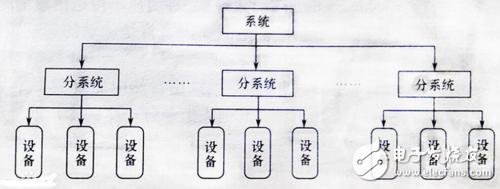
1. Layered design principle of electromagnetic compatibility
This is mainly considered in accordance with the order of electromagnetic compatibility design, which can be divided into the following layers from first to last:
(1) component selection and PCB design, which is critical;
(2) Grounding design, this is the main means. If the above two layers are designed well, more than 80% of the electromagnetic compatibility can be completed.
(3) shielding design;
(4) Filter design and transient disturbance suppression. The above two layers are auxiliary means, mostly after-the-fact remedial measures, which are the least recommended by us.
(5) According to the actual circuit needs, combined with the above layers to comprehensive design.
2, the method of ensuring electromagnetic compatibility
Electromagnetic compatibility is guaranteed from the following aspects mainly based on the three elements that constitute interference.
2.1 Guarantee electromagnetic compatibility at different levels
1) From the component level, when it is a passive component, consider
(1) Component parameters outside the operating band are quite different from those in the operating band;
(2) The end lead of the plug-in component has an inductance, and this inductor is prone to electromagnetic compatibility problems at high frequencies;
(3) The component has parasitic capacitance and parasitic inductance, which is distributed parameter on the circuit. When analyzing the circuit, the equivalent circuit brought by it should also be considered. When it is an active component, the electromagnetic radiation generated in the work will also become a source of interference by conducting current. When it is a nonlinear component, a change in the spectral composition may occur, and this change may also cause interference.
2) From the device level, it is mainly to ensure that the coupling of sensitive devices is reduced.
(1) increase the pulse leading edge time to reduce the interference bandwidth;
(2) Eliminating harmonics generated by the oscillator in the circuit and harmonics of the signal;
(3) Ways to limit interference or eliminate interference.
3) From the system level, it is mainly guaranteed by means of organization or system engineering, because it is possible to improve the electromagnetic compatibility on a single device, but at the same time it affects the working conditions of other devices, making the performance of other devices If the indicator becomes bad, it needs to be compromised from the system. In addition, the important point is that the EMC design must be highly valued by the overall design of the system.
2.2 reduce the coupling between the wires
Mainly from the increase of the distance between the wires, the use of shielding, the use of twisted pair or the use of shielding plus twisting is considered.
2.3 Grounding
Mainly should be considered
(1) The impedance of the grounding conductor and the common line should be the smallest, preferably less than λ/20 of the maximum working frequency of the product;
(2) The grounding conductor shall be a grounding wire with a tubular cross section;
(3) Reliable grounding and prevent the formation of an oxide layer at the connection point;
(4) Use one point of parallel grounding (for low frequency) or multi-point grounding (for high frequency).
2.4 shielding
When it is a low-frequency magnetic field, the magnetic shielding is mainly considered. When the shielding layer is thicker, the higher the conductivity of the material, the better the shielding performance; when it is a high-frequency magnetic field, an electric field or an electromagnetic field, it is mainly considered to be shielded by a thin metal and well grounded. Another thing worth noting is that when the cable is made, the metal casing of the cable shielding layer and the connector plug is required to have a complete 360-degree overlap, and the phenomenon of "pig tail" cannot be seen, otherwise the effect is greatly reduced.
2.5 filtering
Main consideration
(1) suppression of interference outside the operating band;
(2) Eliminating useless spectral components with an absorption filter in the signal circuit;
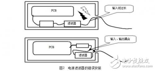
(3) Eliminate the interference generated in the power supply circuit (especially in the switching power supply), the steering circuit, the control circuit, and the conversion circuit. In engineering practice, one of the most notable places is the installation of the power filter. The wrong installation of the common filter is shown in Figure 2.
2.6 Spatial location of electronic equipment
Since the receiving characteristics of various electronic devices and the radiation characteristics of the interference source devices have a certain directivity and a certain working distance, these characteristics can be utilized to appropriately arrange the position of the electronic device in the device space to avoid interference and interference, that is, attention Determine the spatial distance and location pattern between electronic devices.
3, PCB design technologyIn addition to component selection and circuit design, good printed circuit board (PCB) routing is also a very important factor in EMC design. Since the PCB is an inherent component of the system, enhancing electromagnetic compatibility in the PCB layout does not incur additional costs for the final completion of the product, and is also very economical from this point of view.
3.1 pay attention to the bandwidth of electromagnetic compatibility design
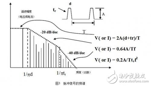
In EMC, in addition to the fundamental frequency, harmonic factors need to be considered, usually taking ten times the frequency, but in digital circuits, such as in the clock circuit and logic gate circuit, the radiation bandwidth and the rising edge of the digital signal or The falling edge is related, not the repetition period of the digital signal, and the relationship is: rtFï°/1max, where rt is the rising edge time of the pulse. For example, the typical clock-driven edge rate is 2 ns. At this time, maxF ≈ 160 MHz, and considering ten times the frequency, this clock circuit may generate a radiation bandwidth up to 1.6 GHz. Therefore, when selecting a device, choose a slow logic device series, because the contribution of the device to electromagnetic radiation is not directly related to the operating frequency and only depends on the edge rate (this is contradictory to the selection of fast devices from the circuit function design. Circuit design needs to be compromised). Also, from the immunity of the device, the CMOS device is the best because of its high noise margin. From the packaging point of view, BGA is the best because its lead is very short. The spectrum of the pulse signal is shown in Figure 3.
3.2 Note that the circuit and circuit schematic for PCB EMC design are different.
Mainly because the PCB schematic diagram does not consider the distribution parameters of components and PCB lines in the circuit, such as distributed inductance, distributed capacitance, distributed mutual inductance, distributed mutual capacitance and transmission delay. For example, a wire is equivalent to a series connection of an inductor and a resistor at a high frequency. The higher the switching speed, the higher the load impedance requirement. The output impedance of the clock driver must be equal to the wave impedance of the clock line. Usually the clock driver must be connected with a series resistor. The empirical value is generally 10 to 30 Ω.
3.3 Pay attention to the principle of PCB layout
(1) The 20-H principle determines the distance between printed lines as follows: All PCBs with a certain voltage will radiate electromagnetic energy to the space (Fig. 4a). To reduce this effect, the physical size of the PCB should be It is 20H smaller than the physical size of the nearest ground plate (where H is the pitch of the two layers of PCB), that is, about 3mm, which can reduce the radiation intensity by 70% (Figure 4b). The schematic diagram of the 20-H principle is shown in Figure 4:
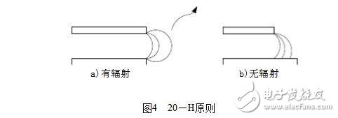
According to the actual engineering experience, using the 20-H rule will greatly increase the self-excited frequency of the PCB.
(2) The 3-W principle, which determines the distance between the power plane and the edge of the PCB, as follows: When the spacing between the two tracks is small, electromagnetic crosstalk occurs between the two lines, causing the circuit to malfunction. To avoid this effect, you should maintain a line width of no less than three times the line width of the line, ie 3W, W is the width of the printed line. The width of the printed lines depends on the requirements of the line impedance.
(3) Ensure that the signal is reliably transmitted on the PCB to ensure signal integrity. The main problems here generally include delay, impedance mismatch, ground bounce, crosstalk and so on. This not only affects the stable operation of the electronic device, but also generates electromagnetic interference. Generally, the delay problem is most easily encountered in high-speed logic design, and undesired processing may cause undesired pulse interference. The effect of the transmission delay on the signal is shown in Figure 5.

3.4 Pay attention to determine the number of PCB wiring layers
First of all, there is an important concept in the design that each wiring layer is preferably adjacent to a real plane (power or ground). in principle:
(1) The power plane should be close to the ground plane and placed below the ground plane. In this way, the capacitance between the two metal plates can be used as the smoothing capacitor of the power supply, and the ground plane can also shield the radiation current of the power supply surface.
(2) The digital circuit is separated from the analog circuit. The digital ground and the simulated ground may not be slotted, but there must be a complete uniform ground plane, and the digital part and the analog part are strictly divided.
(3) The printed lines of the intermediate layer form a planar waveguide, and microstrip lines are formed on the surface layer, and the transmission characteristics of the two are different.
(4) Circuits Especially high-frequency circuits are the main sources of interference and radiation, and must be arranged separately and away from sensitive circuits.
(5) The signal plane should be arranged adjacent to the entire metal plane in order to generate flux cancellation.
(6) The stray current and the high-frequency radiation current contained in different layers are different, and should be treated differently when wiring. Decoupling capacitors can be used for stray currents and by reducing the loop area for high frequency radiated currents.
The following are common PCB layer designs for reference (S for the signal layer, G for the formation, and P for the power plane). Four-layer board: S1, G, P, S2
Six-layer board: S1, G, S2, P, G, S3
Eight-layer board: S1, G, S2, G, P, S3, G, S4
Ten-layer board: S1, G, S2, S3, G, P, S4, S5, G, S6 (but S4 is sensitive to power supply noise)
3.5 pay attention to PCB grounding design
1) First, the concept of distributed parameters is to be established. Above a certain frequency, any metal wire can be regarded as a device composed of a resistor and an inductor. Therefore, the ground lead has a certain impedance and constitutes an electrical loop. Whether it is a single-point ground or a multi-point ground, it must constitute a low-impedance loop. Really or rack.
2) Grounding method
(1) Single point grounding. If the operating frequency of the component is less than 1MHz, single-point grounding is a good way, but when the frequency is increased, the inductance of the connecting line is prominent, and the grounding impedance will rise when the length of the grounding wire is the periodic signal. When it is divided into an odd multiple of one wavelength, not only the impedance is high, but also an antenna that radiates electromagnetic energy.
(2) Multi-point grounding. The high-frequency circuits are grounded at multiple points. At this time, the grounding impedance can be minimized, and the RF current can be shunted from the ground plane to the metal floor, because the low inductance component of the solid metal plate will form a low-impedance loop.
(3) The digital circuit should be treated as a high-frequency analog circuit. It should also be kept low-inductively grounded and grounded using a high-quality decoupling capacitor (0.1 uF in parallel with 0.001 uF and two orders of magnitude difference).
(4) Grounding and signal loop, the RF current always needs to return a road to the starting point. In the electromagnetic compatibility design, the high-speed logic circuit is always placed as close as possible to the bottom plate, and the grounding plate is installed to better reduce the high-frequency radiation. Loop. The length of the ground wire connected to the ground must be very short, as short as λ/20 of the highest working frequency of the product.
(5) Grounding sequence. Since the grounding disturbance (or noise) is generally the largest, it should be connected to the reference ground first (the purpose of this is to let the reference ground absorb the disturbance first), and then send it to analog ground and digital ground. Go up.
3.6 Pay attention to the design of the capacitor in the PCB
Capacitors in EMC can be divided into decoupling capacitors, bypass capacitors, and housing capacitors. The decoupling capacitor is mainly used to filter the radiation current caused by the high frequency device on the power board, to provide a localized DC for the device, and to reduce the peak value of the current surge in the printed circuit. Usually, the ceramic capacitor is used. As a decoupling capacitor, its value depends on the rise time and fall time of the fastest signal. For example, for a 33MHz clock signal, a capacitance of 4.7uF to 100uF can be used. For a 100MHz clock signal, a 10uF capacitor can be used. In addition, engineering The effect of ESR on the decoupling ability should also be considered. Generally, a capacitor with an ESR value lower than 1 ohm is selected. Bypass capacitors can eliminate high-frequency radiation noise. Generally, aluminum electrolytic capacitors and tantalum capacitors are more suitable as bypass capacitors. The capacitance value depends on the transient current requirement on the PCB. Generally, it is in the range of 10-470uF. There are many integrated circuits, high-speed switching circuits and power supplies with long leads, so you should choose a large-capacity capacitor. The accommodating capacitor is used to solve the problem that the power supply voltage will suddenly drop when the switching device operates.
In short, when selecting a capacitor, you should choose not only the temperature coefficient but also a capacitor with a small equivalent series inductance (less than 10nH) and a small equivalent series resistance (less than 0.5Ω). In terms of material, Z5U material is generally selected when it is lower than 50MHz. It has stable performance, large dielectric constant and large capacitance. When it is larger than 50MHz, NPO material is generally selected, and its dielectric constant is small. Usually the engineering practice is to use two capacitors in parallel, one large and one small (capacitance value).
3.7 Pay attention to the design of PCB vias
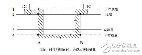
When wiring, try to pass through the hole as little as possible. Because the impedance of the via is different from the impedance of the line, there is a sudden change in impedance, which causes the standing wave to deteriorate the signal, and it is easy to form radiation, especially when the clock needs to be layered. The processing of the clock line across layers is shown in Figure 6.
(end)
Anti-virus disposable safety coverall protective clothing
This product is non-sterile
It can be used in hospital, just hospital staff need to do sterilization before using;
It can effectively resist the penetration of bacteria, viruses, alcohol, blood, body fluids, air dust particles, can effectively
protect wearer from the theat of infection.
Protective Work Clothing,Ebola Protective Clothing,Safety Protective Clothing,Disposable Protective Clothing
Guangzhou HangDeng Tech Co. Ltd , http://www.hangdengtech.com