The ever-increasing switching power supply power density has been limited by the size of passive components. Taking high frequency operation can greatly reduce the size of passive components such as transformers and filters. However, excessive switching losses are bound to become a major obstacle to high-frequency operation. In order to reduce switching losses and allow high frequency operation, resonant switching technology has been developed. These technologies use a sinusoidal approach to power, and switching devices enable soft switching. The switching loss and noise are greatly reduced.
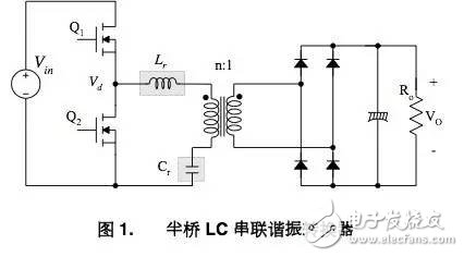
Among the various types of resonant converters, the simplest and most common resonant converter is an LC series resonant converter in which the rectifier-load network is connected in series with the LC resonant network, as shown in Figure 1 [2-4]. In this circuit configuration, the LC resonant network forms a voltage divider with the load. The impedance of the resonant network can be changed by changing the frequency of the driving voltage Vd. The input voltage is divided between the resonant network impedance and the reflected load. Due to the voltage division, the DC gain of the LC series resonant converter is always less than one. Under light load conditions, the load impedance is large compared to the impedance of the resonant network. All input voltages are applied to the load. This makes it difficult to adjust the output under light load. In order to be able to adjust the output at no load, the theoretical resonant frequency should be infinite.
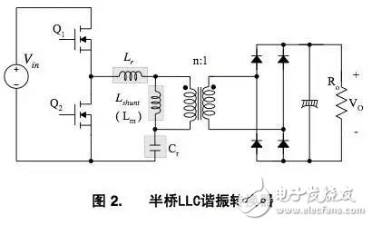
In order to break the limitations of series resonant converters, LLC resonant converters have been proposed [8-12]. The LLC resonant converter is an improved LC series resonant converter that is implemented by placing a shunt inductor in the primary winding of the transformer, as shown in Figure 2. The use of shunt inductors can increase the circulating current of the primary winding, which is beneficial to the operation of the circuit. Since this concept is not intuitive, it has not received enough attention when the topology was first proposed. However, in high input voltage applications where switching losses are dominant compared to on-state losses, efficiency is improved.
In most practical designs, the shunt inductor uses the magnetizing inductance of the transformer. The circuit diagram of the LLC resonant converter is very similar to the circuit diagram of the LC series resonant converter. The only difference is that the values ​​of the magnetizing inductance are different. The excitation inductance of the LLC resonant converter is much larger than the excitation inductance (Lr) of the LC series resonant converter. The excitation inductance in the LLC resonant converter is 3-8 times that of Lr, which is usually obtained by increasing the air gap of the transformer.
LLC resonant converters have many advantages over series resonant converters. It regulates the output over a wide range of power and load fluctuations, while the switching frequency fluctuates less. Zero voltage switching (ZVS) is available throughout the entire operating range. All inherent parasitic parameters can be used to implement soft switching, including junction capacitance, transformer leakage inductance and magnetizing inductance of all semiconductor devices.
Including the explanation of the working principle of LLC resonant converter, the design of transformer and resonant network, and the selection of components. Design examples are given to explain the design process one by one, which is helpful for the design of LLC resonant converters.
LLC resonant converter and fundamental approximation
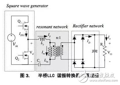
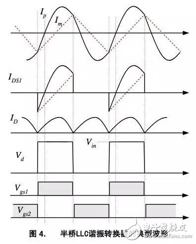
A schematic diagram of the half-bridge LLC resonant converter is shown in Figure 3. In the figure, Lm refers to the magnetizing inductance, which is used as a shunt inductor, Lr refers to the series resonant inductor, and Cr refers to the resonant capacitor. Figure 4 shows a typical waveform of an LLC resonant converter. Assume that the operating frequency is the same as the resonant frequency, which is determined by the resonance between Lr and Cr. Since the magnetizing inductance is relatively small, a considerable amount of exciting current (Im) is formed, which is freewheeling in the primary winding and does not participate in the transmission of electric energy. The primary current (Ip) is the sum of the excitation current and the current reflected from the secondary current to the primary.
In general, the LLC resonant topology consists of a 3-stage circuit, as shown in Figure 3, which is a square wave generator, a resonant network, and a rectifier network.
The square wave generator is responsible for generating the square wave voltage Vd, which is achieved by alternately driving the switches Q1 and Q2 with a 50% duty cycle. Usually, a small dead time is introduced in continuous switching. The square wave generator can be constructed in a full bridge or half bridge type.
• The resonant network consists of a capacitor, transformer leakage inductance, and magnetizing inductance. The resonant network filters out higher harmonic currents. In essence, even if a square wave voltage is applied to the resonant network, only sinusoidal current is allowed to flow through the resonant network. The current (Ip) lags behind the voltage applied to the resonant network (ie, the fundamental component of the square wave voltage (Vd) is applied to the totem pole of the half bridge), allowing the MOSFET to be turned on at zero voltage. As shown in Figure 4, the MOSFET turns on when the MOSFET voltage is zero, at which point the current flows through the anti-parallel diode.
• The rectifier network generates a DC voltage and uses a rectifier diode and a capacitor to rectify the AC. The rectifier network can be designed as a full-wave rectifier bridge or center-tapped configuration with a capacitive output filter.
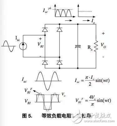
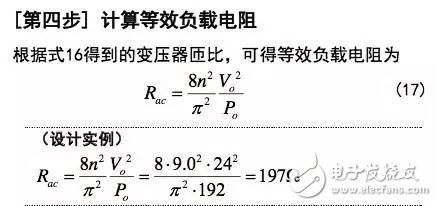
The filtering effect of the resonant network can be obtained by the fundamental approximation principle, and the voltage gain of the resonant converter is obtained. It is assumed that the fundamental component of the square wave voltage is input to the resonant network and the electrical energy is transmitted to the output. Since the secondary side rectifier circuit can be used as an impedance transformer, its equivalent load resistance is not the same as the actual load resistance. Figure 5 shows the derivation of this equivalent load resistance. The primary circuit is replaced by a sinusoidal current source Iac, which appears at the input of the rectifier. Since the average value of |Iac| is the output current Io, Iac can be described as
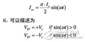
Note: Vo refers to the output voltage.

Since the harmonic components of the VRI do not involve power transmission, the AC equivalent load resistance can be calculated using (VRIF/ Iac):
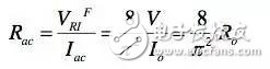
Considering the transformer turns ratio (n=Np/Ns), the primary equivalent load resistance can be
Described as

AC equivalent circuit can be obtained by using equivalent load resistance, as shown in Figure 6.
FF
As shown, Vd and VRO in the figure refer to the fundamental component of the driving voltage Vd and the reflected output voltage VRO (nVRI), respectively.
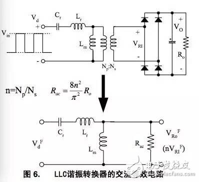
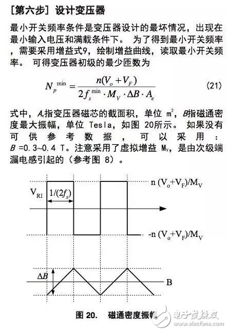
Using the equivalent load resistance obtained in Equation 5, the characteristics of the LLC resonant converter can be derived. Using the AC equivalent circuit shown in Figure 6, the formula for calculating the voltage gain M can be obtained:
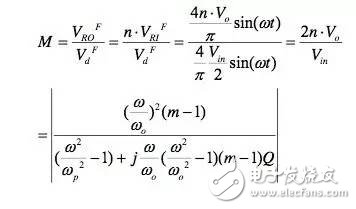
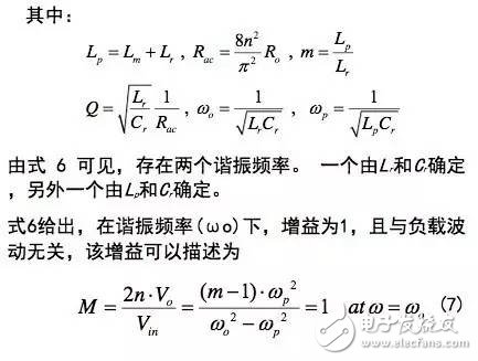
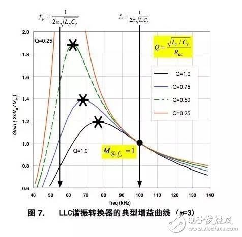
Figure 7 shows the difference in Q values ​​and m=3, fo=100kHz and fp=57kHz
The gain expressed by Equation 6 is expressed. As can be seen from Figure 7, the LLC resonant converter exhibits a voltage gain characteristic that is almost independent of the load when the switching frequency is near the resonant frequency fo. This is an outstanding advantage of the LLC type resonant converter over traditional series resonant converters. Therefore, it is assumed that the converter operates near the resonance frequency, reducing the switching frequency fluctuation.
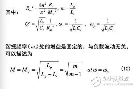
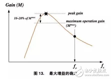
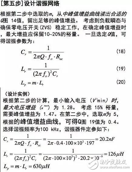
The operating range of the LLC resonant converter is subject to peak gain (up to maximum gain), which is labeled '*' (as shown in Figure 7). It should be noted that the peak voltage gain does not appear near fo or fp. The frequency at which the peak voltage gain is obtained is between fp and fo, as shown in FIG. As the load becomes lighter, the Q value decreases, the peak gain frequency shifts to fp, and the peak gain decreases. Therefore, for resonant network design, the full load condition is the worst case.
Integrated transformer considerations
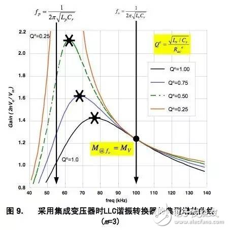
For the actual design, it is usually necessary to implement the magnetic device (series inductance and shunt inductance) using the concept of an integrated transformer, in which the leakage inductance is used as a series inductance and the excitation inductance is used as a parallel inductance. When the magnetic element is constructed by this method, it is necessary to improve the equivalent circuit in Fig. 6 to Fig. 8 because there is a leakage inductance not only at the primary but also at the secondary. Failure to consider the leakage inductance of the transformer secondary often leads to design errors.
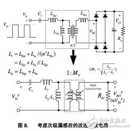
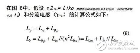
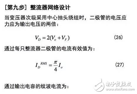
When dealing with actual transformers, it is advisable to use equivalent circuits with Lp and Lr, since these inductance values ​​can be easily measured at the primary by separately opening and shorting the secondary windings. In the actual transformer, Lp and Lr can be measured on the primary side under the condition that the secondary winding is open and shorted, respectively.
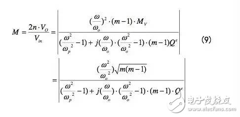
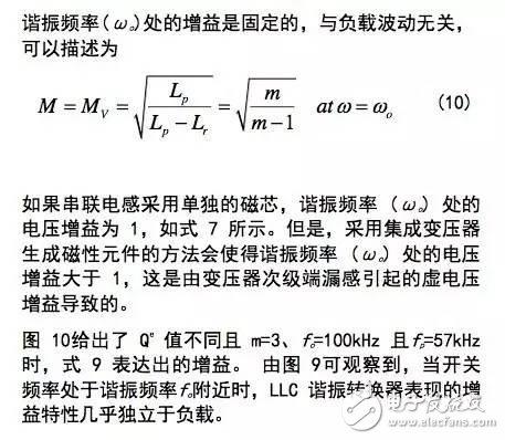
In Figure 9, a virtual gain MV is introduced, which is caused by the leakage inductance of the secondary side. Using the improved equivalent circuit of Figure 9, the gain expression of Equation 6 can be adjusted to obtain the gain expression of the integrated transformer:
Working mode and maximum gain considerations
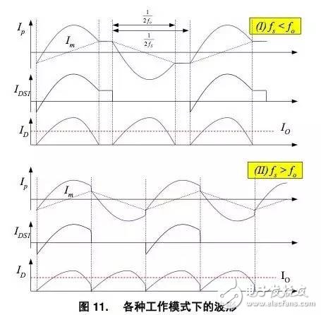
The LLC resonant converter can operate at a lower or higher resonant frequency (fo), as shown in Figure 10. Figure 11 shows the current waveforms of the primary and secondary transformers for each mode of operation. Operating below the resonant frequency (Case I) allows the secondary rectifier diode to achieve soft commutation, although the loop current is larger. As the operating frequency decreases and deviates from the ID resonant frequency, the circulating current is greatly increased. Although operating at higher than the resonant frequency (Case II) allows for a reduction in the circulating current, the rectifier diode cannot achieve soft commutation. For high output voltage applications, such as plasma display panels (PDPs), it is recommended to operate below the resonant frequency because the reverse recovery losses of the rectifier diodes in this type of application are comparable.
Big. Operating below the resonant frequency, it also has a narrower frequency range for load fluctuations, because its operating frequency is limited below the resonant frequency even when operating under no-load conditions.
On the other hand, when operating in the upper resonance, the on-state loss is smaller than when operating in the lower resonance. For low output voltage applications, such as liquid crystal display (LCD) TV or laptop adapters, good efficiency is exhibited. Because of this type of application, the secondary rectifier diode is suitable for Schottky diodes, and the reverse recovery problem is irrelevant. However, when operating at the upper resonant frequency, operating at light loads causes a large increase in switching frequency. When the upper resonance works, the frequency jump function is needed to prevent the switching frequency from rising sharply.
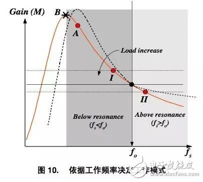
Maximum gain and peak gain requirements Â
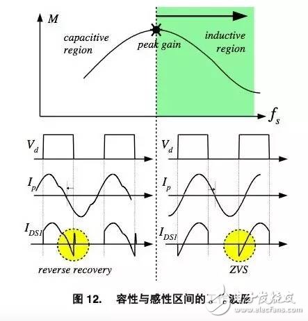
Above the peak gain frequency, the input impedance of the resonant network is inductive, and the input current (Ip) of the resonant network lags behind the voltage (Vd) applied to the resonant network. Thus the MOSFET can achieve zero voltage turn-on (ZVS), as shown in Figure 12. Show. Below the peak gain frequency, the input impedance of the resonant network is capacitive, and Ip leads Vd. When operating in the capacitive range, during the switching process, the body diode of the MOSFET is reversely recovered, causing severe noise. Another problem with entering the capacitive range is that the output voltage is out of control due to the inverse of the gain slope. The minimum switching frequency should be appropriately higher than the peak gain frequency
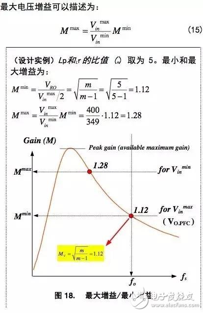
The appropriate input voltage range for the LLC resonant converter is determined by the peak voltage gain. Therefore, the resonant network should be designed to ensure that the gain curve has sufficient peak gain and can cover the entire input voltage range. However, below the peak gain point, the ZVS condition is lost, as shown in Figure 12. Therefore, when determining the maximum gain point, it is required to reserve some margin, ensuring stable ZVS operation during the load transient and startup phases. Typically, for the actual design, 10-20% of the maximum gain is selected as the margin, as shown in FIG.
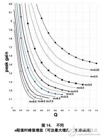
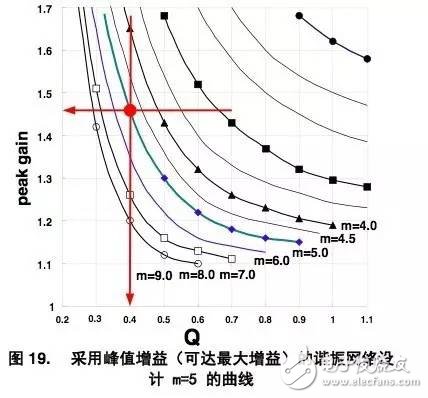
Under a given condition, even if the peak gain is obtained using the gain formula 6, it is difficult to express the peak gain in a clear form. To simplify analysis and design, a simulation tool can be used to obtain the peak gain, as shown in Figure 14. The figure shows the peak gain (up to the maximum gain) as the value of Q changes for different values ​​of m. It can be seen that by reducing the m and Q values, a higher peak gain can be obtained. For a given resonant frequency (fo) and Q value, decreasing m means that the magnetizing inductance is reduced, which will result in an increase in the circulating current. Naturally, a trade-off should be made between the available gain range and the conduction loss.
Characteristics of the FSFR series
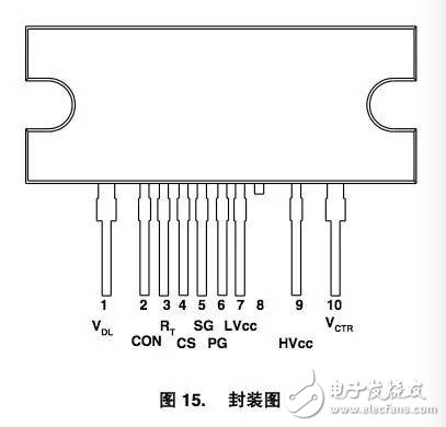
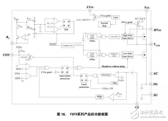
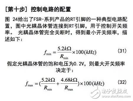
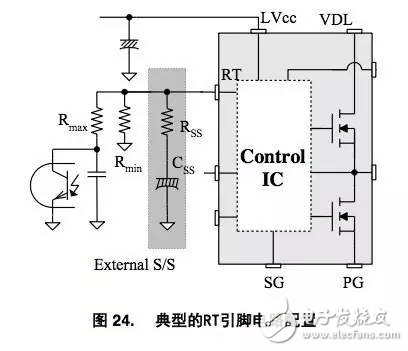
The FSFR family integrates a pulse frequency modulation (PFM) controller and a MOSFET specifically designed for zero voltage switching (ZVS) half-bridge converters with minimal external components. The internal controller includes an undervoltage lockout, an optimized high-side/low-side gate driver, a temperature-compensated precision current-controlled oscillator, and a self-protection circuit. Compared to discrete MOSFET and PWM controller solutions, the FSFR family reduces total cost, component count, size and weight while increasing efficiency, productivity and system reliability.
Design steps
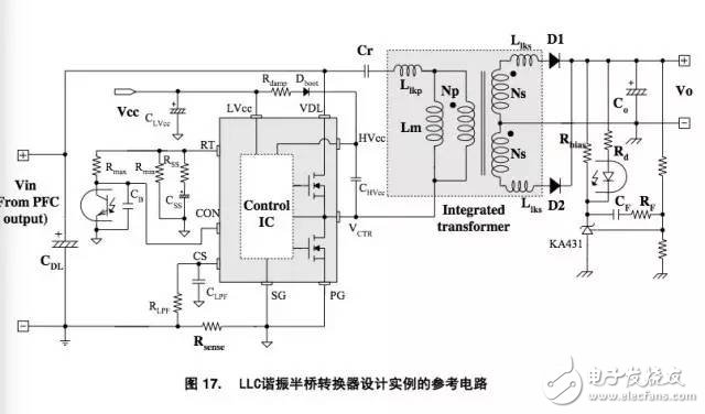
This section provides design steps based on the schematic shown in Figure 17. The integrated transformer has a center tap and the input voltage comes from a pre-regulator-power factor corrector (PFC). A DC/DC converter with a 192W/24V output has been selected as a design example. The design specifications are as follows:
- Nominal input voltage: 400VDC (PFC stage output) - Output: 24V/8A (192W)
- Hold time requirement: 20 milliseconds (50Hz power frequency)
- PFC output DC capacitor: 220μF
[[STEP-1] Determining the various indicators of the system
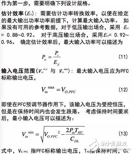
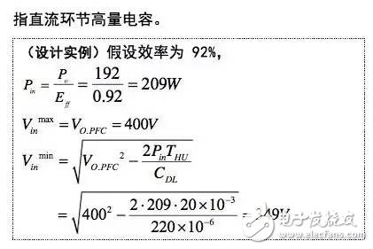
[[STEP-2 determines the maximum and minimum voltage gain of the resonant network
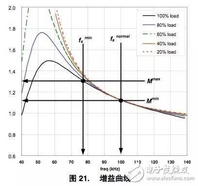
According to the discussion in the previous section, in order to reduce switching frequency fluctuations, the LLC resonant network should typically be designed to operate near the resonant frequency (fo). Since the LLC resonant converter is powered by the PFC output voltage, the PFC nominal output voltage should be accommodated in order to design the operating frequency of the converter at fo.
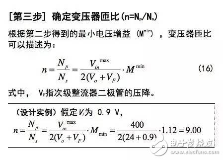
As can be seen from Equation 10, the gain at fo is a function of m (m = Lp / Lr). The gain at fo is determined by the choice of m values. Although a high peak gain can be obtained when the value of m is small, an excessively small value of m causes a deterioration in the coupling of the transformer and a decrease in efficiency. Typically, setting m to 3 to 7 allows the voltage gain at the resonant frequency (fo) to be 1.1 to 1.2.
After the value of m is selected, the voltage gain at the nominal output voltage of the PFC can be described as:


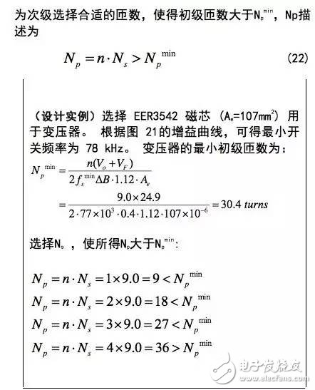
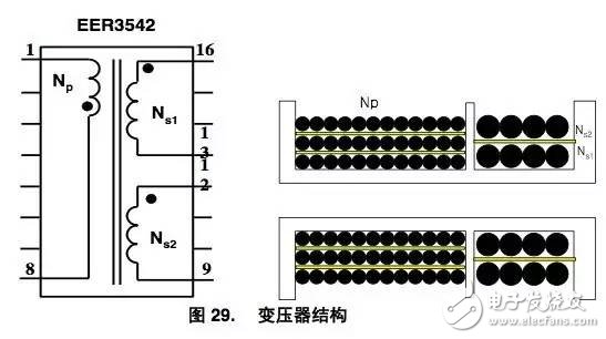
- Core: EER3542 (Ae=107 mm2)
- Skeleton: EER3542 (horizontal/segment type)
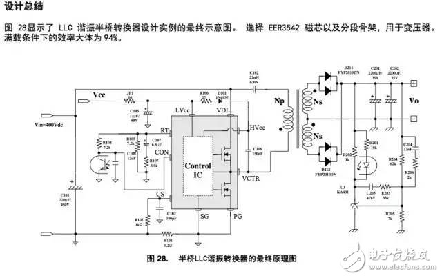
6. Experimental verification
In order to verify the validity of the design process in this instruction manual, the converter design example was built and tested. All circuit components involved in the design example have been adopted.
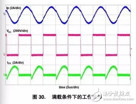
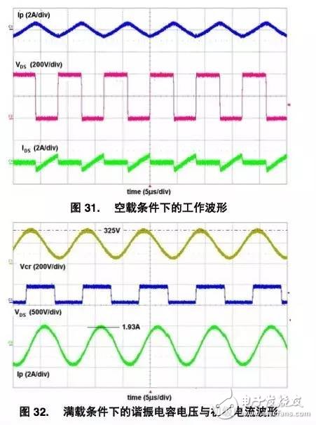
Figure 30 and Figure 31 show the operating waveforms at full load and no load for the nominal input voltage. It can be seen that due to the resonance effect, the drain-source voltage (VDS) of the MOSFET drops to zero before turn-on, achieving zero voltage switching.
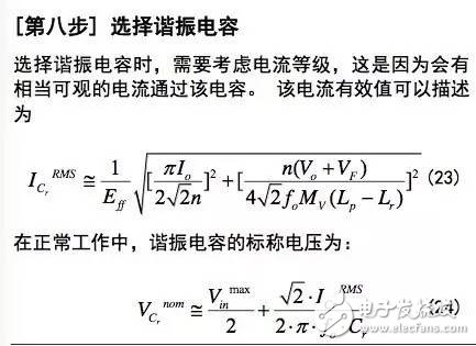
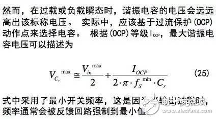
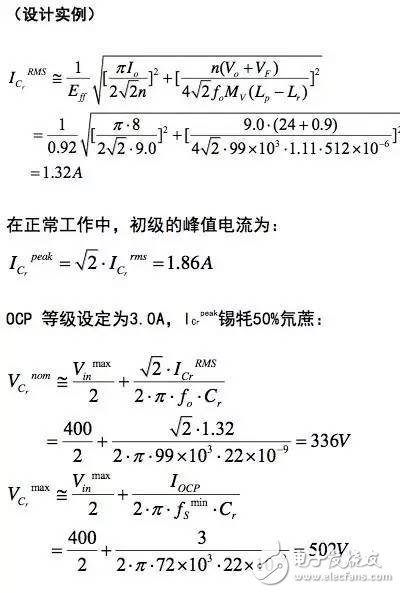
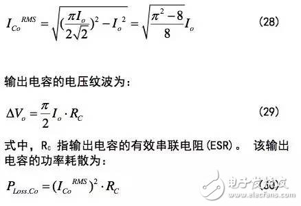
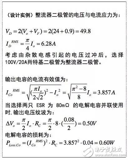
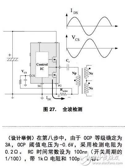
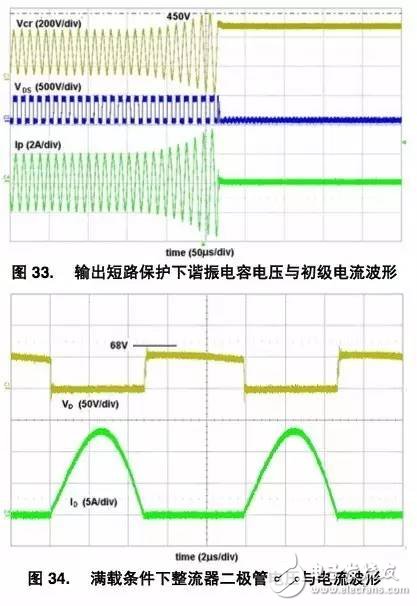
Figure 32 shows the resonant capacitor voltage and primary current waveform at full load. The peak value of the resonant capacitor voltage and the primary side current are 325V and 1.93A, respectively, which closely matches the calculated value of the eighth step in the design process chapter. Figure 33 shows the resonant capacitor voltage and primary side current waveform for an output short circuit condition. For the output short-circuit condition, when the primary current is greater than 3A, the overcurrent (OCP) acts. The maximum voltage of the resonant capacitor is slightly higher than the calculated value of 419V, because the 1.5μs turn-off delay makes the OCP operating current slightly higher than 3A (refer to the FSFR2100 product specification).
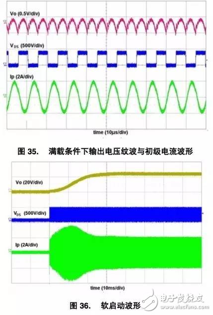
Figure 34 shows the voltage and current waveforms of the rectifier diodes under full load and no load conditions. The voltage stress is slightly higher than the calculated value in the ninth step due to the voltage overshoot caused by the stray inductance. Figure 35 shows the ripple waveform of the output voltage under full load and no load conditions. The ripple of the output voltage matches the design value in the ninth step.
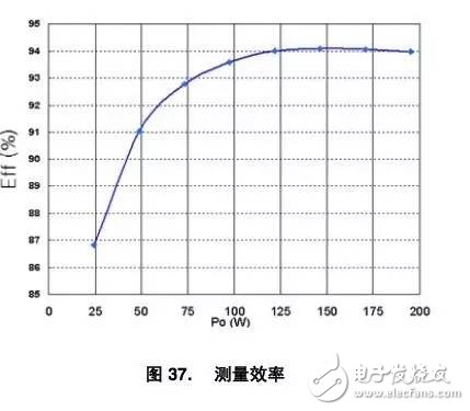
Figure 36 shows the efficiency measurements for different load conditions. The efficiency at full load is approximately 94%.
Graphic I network
5.1 Home Theater Speaker,Home Theatre 5.1,Wireless Surround Sound Speakers,Bluetooth Surround Sound System
GUANGZHOU SOWANGNY ELECTRONIC CO.,LTD , https://www.jerry-power.com