Three implementations of OLED screen color
The "evaporation" method of the high-end atmosphere mentioned below is mainly applied to a typical OLED screen of RGB three-color arrangement. Many of Samsung's OLED TV products are based on this method, and the effect is very good. The three primary colors are very pure, but the cost is very high. The technique used in this type of vapor deposition is called FMM, a fine metal mask, which is to cover the pixels and cover a mask during evaporation, so the alignment problem and the mask material itself become technical difficulties.
In fact, in order to control costs, humans have more than one kind of OLED TV. There is a type of blue light + color conversion layer: this scheme only needs to evaporate blue OLED components, and converts the light into RGB three colors through the conversion layer. The limitations of converter development have not been adopted on a large scale.
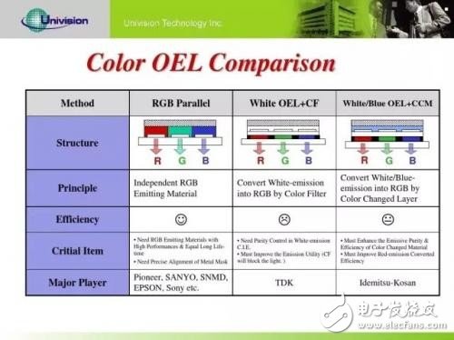
There is also a class of OLED TVs that are white light + three color filters, which are similar in principle to LCD liquid crystal panels, with white backlighting and color filters - this method is obviously much lower in cost, LG OLED TVs have been produced in this way. White OLEDs + color filters have also been considered as OLEDs to further realize low-cost solutions. Only with the addition of filters, the light color purity is more problematic, so the brightness, contrast, color, and energy saving performance are theoretically inferior to RGB OLED.
AMOLED flat panel display development process and technical difficulties
The development of AMOLED technology mainly involves two aspects of TFT backplane and OLED device. In the choice of technical routes, there is currently no international unification, and a variety of technical solutions are under development.
The performance of the OLED, ie OLED, determines the color performance and power consumption of the AMOLED display. Therefore, the development of OLED device technology is of great significance to the improvement of product competitiveness. There are two key points in OLED device fabrication technology. One is to develop high mobility transmission materials and high efficiency, long life luminescent materials, and the other is to develop new device structures and improve device performance. Therefore, the development of new organic materials, the design of new device structures and the improvement of vacuum evaporation technology will be the focus of research.
At present, the channel layer semiconductor material in the TFT backplane mainly includes amorphous silicon (a-Si), microcrystalline silicon (μ-Si), low temperature polysilicon (LTPS), single crystal silicon, organic matter and oxide. Since the OLED is a current-driven device, a stable current is required to control the luminescence characteristics. In order to achieve sufficient brightness, AMOLEDs require higher channel mobility of the TFT channel material to provide higher current density. Therefore, amorphous silicon TFTs currently commonly used in TFT-LCDs are difficult to meet due to low mobility. Claim. In addition, unlike the TFT-LCD, the AMOLED requires the TFT to be turned on for a long time, and the threshold voltage drift problem of the amorphous silicon TFT makes it difficult to apply to the AMOLED. From the current state of technology development, more promising technologies are LTPS TFT and oxide TFT, but there are also many difficulties.
At present, the most mature TFT backplane technology used in AMOLED is low temperature polysilicon (LTPS) technology. In the LTPS technology, the most important process difficulty is the preparation of the polysilicon channel layer. In the process, a layer of amorphous silicon is first deposited on a glass substrate containing no alkali ions by means of PECVD, and then the amorphous silicon film is absorbed by laser or non-laser, and the atoms are rearranged to form a polysilicon structure. Reduce defects and get higher electron mobility.
For LTPS crystallization technology, laser crystallization technology, especially excimer laser annealing (ELA) technology, is now mature in small-size applications. The global production of AMOLED products has basically used ELA technology. The difficulty of ELA technology lies in the consistency problem of TFT. The difference in TFT characteristics between pixels leads to uneven illumination intensity of OLED, which leads to the inconsistency of panel yield. Therefore, the TFT consistency prepared by ELA technology has been the unit at home and abroad. The focus of research and development. In addition, ELA technology also has a large problem in mass production of large-sized substrates.
On the other hand, non-laser crystallization technology has great advantages in mass production of large-sized substrates and cost reduction, as well as in TFT uniformity. However, non-laser crystallization technology also has technical problems at this stage. Metal-induced crystallization (MIC) technology is difficult to solve defects and lifetime problems due to leakage current caused by metal contamination; solid phase crystallization (SPC) technology has a large comprehensive advantage in the preparation of large-size AMOLEDs. However, its carrier mobility is lower than that of laser crystallization technology, and it still needs further improvement in mass production technology.
AMOLED production process
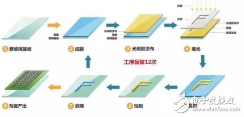
The manufacturing process of LTPS-AMOLED includes many cutting-edge technologies in the display panel industry, which are mainly divided into three processes: back plate segment, front plate segment and module segment. The back plate segment process forms a film of different materials of different patterns by film formation, exposure, etching to form an LTPS (low temperature polysilicon) driving circuit, which provides a lighting signal and a stable power input for the light emitting device. The technical difficulties are the micron-level process fineness and the extremely high uniformity requirements for electrical specifications.
The coating process is to use a coating device to physically or chemically deposit the desired material onto the glass substrate (2);
The exposure process is to use optical illumination to transfer the pattern on the reticle to the coated substrate (3, 4, 5) through the photoresist;
The etching process is to etch away the film under the pattern not covered by the photoresist on the substrate by chemical or physical means, and finally the photoresist on the cover film is washed away, leaving a film layer with the desired pattern (7, 8). ).
Medical Training Media Processor
Medical Training Media Processor,Medical Video Recorder,Video Conferencing Encoders,Medical Signal Recording Encoders
SZ REACH TECH,.CO LTD , https://www.szreachtech.com