It is well known that when the output of the power supply exceeds the rated load or short circuit, it will cause damage to the power supply, resulting in the system not working properly. For this purpose, we have to design the power supply for current limiting protection. So there are many ways, we can design him to the input of the power supply or to the output of the power supply. To achieve the best design method depends on the actual situation, the following methods are commonly used current control methods:
1), the primary reference direct drive mode power supply can be designed to the input, as shown below
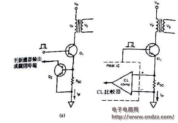
The working principle of the two circuits in Figure 1 is:
(a) Figure: When an overload or short circuit occurs at the output, the primary current will increase rapidly, and a voltage will be generated on the Rsc. If this voltage exceeds the turn-on voltage of BE, Q2 will turn on. The potential of the Q2 collector will be pulled to the ground. If the oscillating circuit is connected, it will lead to the oscillating circuit to stop working, thus achieving the purpose of protection.
The value of Rsc is: Rsc=Vbe/Ip
(b) The circuit in the figure is a commonly used current limiting protection circuit that is popular with designers in counterattack or forward circuits. His work process is somewhat similar to the work process of (a), but he has some good advantages.
First, the comparator's current-limited excitation threshold voltage can be pre-fabricated to an accurate and pre-fabricated level, which is equivalent to the threshold voltage of the bipolar transistor with a larger Vbe voltage range, followed by the threshold. The voltage is small enough, basically 100 MV and 200 MV, so the current limiting power pack can be smaller, which can improve efficiency.
2) Current limiting circuit applied to the base driver
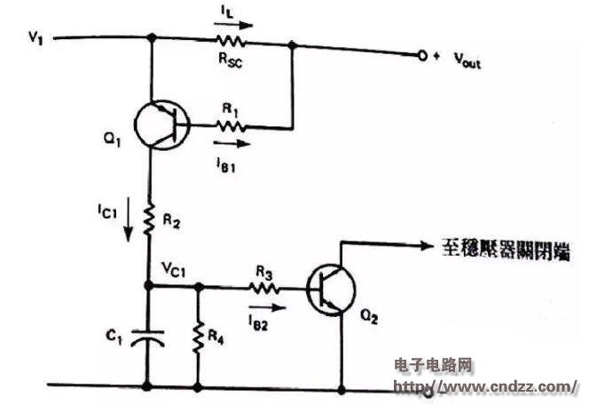
The current limit circuit diagram drawn in the above figure is suitable for the power supply of various circuits. The output portion of such a circuit is co-located with the control circuit.
The working principle is: Under normal working conditions, Il flowing into Rsc will not generate a large voltage drop, then Q1 will not be turned on. If the load current is large enough, voltage will be generated on Rsc, so that Q1 Turn on. If Q1 is in the OFF state, and C1 will be completely discharged when Ic1=0, Q2 will also be in the OFF state. If the Il current is gradually increased, then Il*Rsc=VbeQ1+Ib1R1
At this time, the collector will have a current Ic1 flowing, and the following time constant will charge C1 T=R2*C1
Then the voltage on C1 is: Vc1=Ib2R3+VbeQ2
In order to minimize the load effect of the capacitor voltage, we can use a Darling stool tube with a higher HFE instead of Q2, so that the base current can be limited to microamperes, and our gate should choose the resistor R4. Far greater than R3. This way, when the current is overloaded, the C1 capacitor will discharge quickly.
The value of R2 is as follows:
IBL=(V1-VBEQ1)/R1
And Ic1=HfeQ1IBLMAX
So, R2"=(V1-VCEMAX)R1/(V1-VBEQ1)
In proper circuit design, VCE can quickly reach its voltage value and bias the Q2 transistor to the on state, which can turn off the regulator's drive signal.
When the overload is removed, the circuit will automatically return to the working state. If an IC PWM control circuit with a fixed current limit comparator is used, then in the circuit of Figure 1B, we put the current limit resistor RSC on the positive side of the output to achieve good current limiting.
Both of the above methods work well in detecting current conditions. However, the presence of the power resistor RSC may become undesired, especially at high current output, which will cause power consumption and affect the efficiency of the whole machine. For the second time, there will be another way to overcome this problem. That is to use a transformer to detect overcurrent. And the components in the circuit that do not consume power, as shown in the figure, the working principle is: T1 is used to detect the load current IL, so the resistor R1 will have a proportional voltage. D3 is a rectifier diode, R3 C1 rectified filter circuit, if current overload occurs, the voltage on capacitor C1 will increase to the conduction voltage of Zener diode Z1, at this time transistor Q1 will conduct, so Q1 collector The signal can turn off the drive signal of the regulator.
It should be noted that the design of T1, the choice of materials should use the ferromagnetic and MPP ring core, but the core can not work in saturation, the design of the number of turns: the number of primary turns is generally selected, the number of secondary turns The choice of the right secondary voltage is determined by NP/NS=IS/IP
Since IR=VS/R1
Therefore, in the case of the maximum specified load current IC, the number of secondary turns must be able to produce the desired voltage value on capacitor C1, so NS = NP * IRR / (Vs + Vd3)
At this point, our door can be wound into a precise transformer, and the actual circuit test must be slightly adjusted in the number of turns in order to achieve the best performance.
There is also a current limiting circuit: as shown in the figure, whether it is placed at the input or output of the power supply can achieve a good effect, the same circuit can also be suitable for multi-output power supply, but there are One point, for each group of outputs to achieve the respective current limit can achieve its role, it takes a lot of effort,
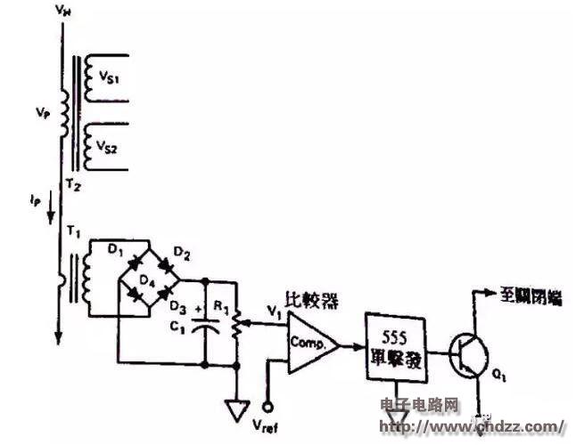
The working principle of the above figure is:
T1 is used to detect the primary current of T2. After T1, the capacitor is filtered by diode rectification. The variable resistor R1 is used to set the threshold voltage at the input of the comparator. In the case of positive long operation, the voltage of the Vref reference input of the comparator will be Higher than the voltage on the R1 of the electric guard, the output of the comparator will be at the high level. At this time, the 555IC (single-excited multivibrator) will have a low level output, so that Q1 will remain in the off state.
If the overload occurs, the voltage V1 will be higher than VREF, so that the comparator is at the bottom potential. The conversion process from the high potential to the bottom potential at the input of IC555 will produce a single-excitation output at the output of IC555, and will be Q1 ON, C-pole. Connected to the closed input or to the soft start capacitor of the PWM circuit, it will pull to ground. The output switching pulse is terminated, and the regulator is turned off. If the over-carrying condition continues, the power supply will be in a dozing state, that is, it will be between the ON and OFF states of the IC555 single-excitation RC time constant period, The conversion is stopped until the overload is removed, and the circuit will resume to return to the normal state.
PCB bus slot edge card sol: 1.27mm, 2.54mm, 3.175mm, 3.96mm, 90 degree, 180 degree dip plug-in board, SMT board, press type, welding type, ear, long pin series.
PCB bus slot edge card sol: 1.27mm, 2.54mm, 3.175mm, 3.96mm, 90 degree, 180 degree dip plug-in board, SMT board, press type, welding type, ear, long pin series
EDGE CARD SOLT
ShenZhen Antenk Electronics Co,Ltd , https://www.antenksocket.com