Abstract: "VCXO" (Voltage Controlled Crystal Oscillator) is an oscillator whose oscillation frequency is determined by the crystal, and the frequency can be adjusted within a small range with a control voltage. VCXO clock (CLK) generator has been applied in various systems, such as digital TV, digital audio, ADSL and STB. This application note describes the structure of VCXO CLK generator, key parameter measurement, PCB design guidelines, and test results of a MAX9485 VCXO CLK generator applied to MPEG2 and AC-3 audio equipment.
VCXO CLK generator structure and application "VCXO", that is, voltage-controlled crystal oscillator, its oscillation frequency is determined by the crystal, but the frequency can be adjusted within a small range with the control voltage, the control voltage range is generally 0V to 2V or 0V to 3V. The tuning range of VCXO is ± 100ppm to ± 200ppm. Figure 1 is a typical VCXO CLK generator structure and crystal oscillator circuit model.
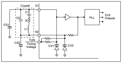
Figure 1. Structure diagram of a typical VCXO CLK generator
Variations in the capacitance of varactor diodes CV1 and CV2 will affect the crystal oscillator model and thus change the oscillation frequency. Two external parallel capacitors CS1 and CS2 are used to adjust the resonance range and center frequency offset. According to the crystal oscillator circuit shown in Figure 1, the resonance frequency can be expressed by the following formula:
Where CL is the equivalent load capacitance determined by CV1,2 and CS1,2. It can be accurately expressed as: CL = (CV1 + CS1) || (CV2 + CS2). Taking the first order approximation and considering C1 << C0 and CL, the frequency increment of fC can be obtained.
Figure 2 is a typical graph of the change of fC with the value of CS1 when CS1 = CS2.
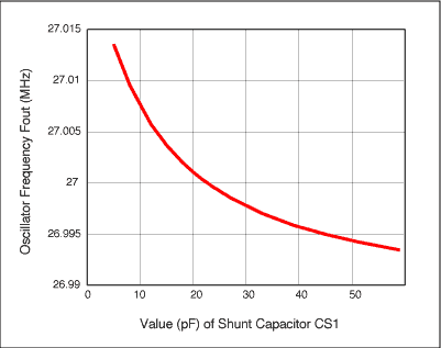
Figure 2. VCXO frequency and parallel capacitor CS1 (CS1 = CS2)
Using this fine-tuning feature, VCXO and PLL can be used to form a CLK generator with fine-tuning features.
VCXO CLK has been applied in various systems, such as digital TV, digital audio, ADSL and STB. Maxim's MAX9485 is such a CLK generator chip, designed specifically for MPEG-2 and Dolby Digital Audio (AC-3) applications [1], it can provide almost all frequencies used in digital audio to analog conversion, supports from Sampling frequency from 12kHz to 96kHz. Maxim has also designed various VCXO CLK generators for other applications.
Key parameters of VCXO CLK generator There are many parameters used to describe VCXO CLK generator. The most important of these are the tuning voltage range, center frequency, pulling range, and clock output jitter.
The tuning voltage range is the variation range of the VCXO control voltage. This voltage controls the capacitance of the varactor diode. Usually 0V to 2V or 3V. The center frequency is the midpoint of the VCXO output frequency range. The traction range is the ratio of the changing frequency (increasing or decreasing) to the center frequency. This ratio is generally expressed in ppm (parts per million) and represents the relative frequency pulling range of VCXO. The traction range is usually about 100 ppm to 200 ppm, depending on the structure of the VCXO and the crystal selected.
Clock jitter is an important parameter of the CLK generator, and there are various definitions of jitter. The two most commonly used jitter parameters are called "cycle" jitter and "inter-cycle" jitter. We will discuss these issues in detail in Section 4. Jitter depends on the structure of the CLK generator, and there will be differences between the chips. Different applications have different requirements for jitter.
Crystal selection and circuit board design Crystal selection and PCB layout will have a certain impact on the performance parameters of the VCXO CLK generator. When choosing a crystal, in addition to frequency, packaging, accuracy, and operating temperature range, attention should be paid to the equivalent series resistance and load capacitance in VCXO applications. The series resistance causes the power consumption of the crystal to increase. The lower the resistance, the easier the oscillator will start. The load capacitance is an important parameter of the crystal. First, it determines the resonant frequency of the crystal. The nominal frequency of a general crystal refers to its resonance frequency after a specified load capacitance is connected in parallel. It should be noted that the nominal frequency here is the value calculated using equation (1) when CL is equal to the specified load capacitance, but not the calculated value 1 / (2 π √L1C1). Therefore, the tuning range of VCXO is closely related to the value of CL. When the load capacitance value is small, the tuning range of the VCXO is limited to the upper end; similarly, when the capacitance value is large, the tuning range will be limited to the lower end. The appropriate value of load capacitance depends on the characteristics of VCXO. For example, in the MAX9485 design, in order to balance the tuning range, the midpoint of the tuning curve, and at the same time simplify the circuit board design, we chose Ecliptek (ECX-5527-27) [2] 27MHz crystal with 14pf load capacitance. When using such a crystal, the MAX9485 has a traction range of ± 200ppm, see Figure 3. It should be noted that packaging will cause differences in the crystal pulling range. The general metal shell package has a larger traction range than surface mount devices (SMD). However, a new SMD crystal produced recently by DAISHINKU Corp. [5] can achieve a traction range similar to that of metal shell crystals. We tested this SMD crystal (DSX530GA), and found that when connecting two parallel capacitors of 4pf, a frequency traction range of ± 200ppm can be achieved, as shown in Figure 4.
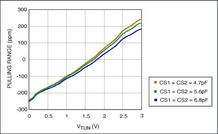
image 3.
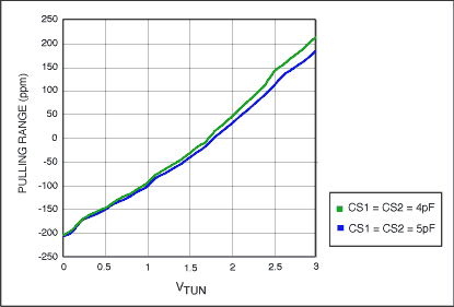
Figure 4.
In order to limit the tuning range of the VCXO, the upward adjustment range can be set by changing the external parallel capacitor. The parallel capacitor value range is 4ps to 7ps, depending on the board parasitic capacitance. On the other hand, the downward adjustment range depends on the value of the internal varactor diode and cannot be changed externally. In order to reduce the influence of the parasitic capacitance on the upward frequency adjustment range, the parasitic capacitance of the crystal pin to the ground should be reduced as much as possible in the circuit board layout to ensure the cleanliness between the pin and the ground layer and the power layer. For detailed circuit board layout, please refer to the MAX9485 evaluation board [4].
The device that measures the output clock jitter is an important performance parameter for oscillators. There are two most commonly used definitions of jitter: periodic jitter and inter-cycle jitter. See Figure 5 for details. In order to measure jitter, a high-speed digital oscilloscope can be used to sample a batch of data and calculate the jitter according to the definition. Tektronix's oscilloscope (TDS 7254) or Lecroy's oscilloscope (Wavepro 960) both provide this type of measurement software. We can also use high-speed digital oscilloscopes to measure period jitter in the time domain [3]. Figure 5 is a device diagram. Jitter cannot be measured between cycles in the time domain. However, if the jitter noise in each cycle is independent and evenly distributed, the jitter between cycles is 1.414 times the period jitter. The MAX9485 can produce 21 different output frequencies, depending on different audio sampling frequencies and frequency scaling factors. We used the equipment shown in Figure 6 to measure the period jitter of various possible output clock frequencies. Table 1 shows the measurement results.
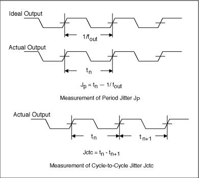
Figure 5. Output jitter measurement
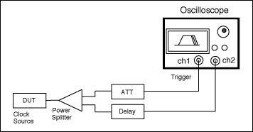
Figure 6. Self-triggered jitter measurement device
Table 1. Periodic jitter and output frequency
As can be seen from the table, in general, the higher the frequency, the lower the jitter. But if we use relative parameters to describe jitter, such as unit interval (UI), see the last column of the table, the jitter is comparable. In addition, it can be noticed that the output frequencies 36.864MHz, 33.8688MHz, 24.5760MHz and 12.288MHz can be realized by different sampling frequencies and scale factors, which results in different jitter values. Therefore, when using these frequencies, the user can obtain the lowest jitter by selecting different Fs and scaling factors.
VCXO CLK generator structure and application "VCXO", that is, voltage-controlled crystal oscillator, its oscillation frequency is determined by the crystal, but the frequency can be adjusted within a small range with the control voltage, the control voltage range is generally 0V to 2V or 0V to 3V. The tuning range of VCXO is ± 100ppm to ± 200ppm. Figure 1 is a typical VCXO CLK generator structure and crystal oscillator circuit model.
Figure 1. Structure diagram of a typical VCXO CLK generator
Variations in the capacitance of varactor diodes CV1 and CV2 will affect the crystal oscillator model and thus change the oscillation frequency. Two external parallel capacitors CS1 and CS2 are used to adjust the resonance range and center frequency offset. According to the crystal oscillator circuit shown in Figure 1, the resonance frequency can be expressed by the following formula:
Where CL is the equivalent load capacitance determined by CV1,2 and CS1,2. It can be accurately expressed as: CL = (CV1 + CS1) || (CV2 + CS2). Taking the first order approximation and considering C1 << C0 and CL, the frequency increment of fC can be obtained.
Figure 2 is a typical graph of the change of fC with the value of CS1 when CS1 = CS2.
Figure 2. VCXO frequency and parallel capacitor CS1 (CS1 = CS2)
Using this fine-tuning feature, VCXO and PLL can be used to form a CLK generator with fine-tuning features.
VCXO CLK has been applied in various systems, such as digital TV, digital audio, ADSL and STB. Maxim's MAX9485 is such a CLK generator chip, designed specifically for MPEG-2 and Dolby Digital Audio (AC-3) applications [1], it can provide almost all frequencies used in digital audio to analog conversion, supports from Sampling frequency from 12kHz to 96kHz. Maxim has also designed various VCXO CLK generators for other applications.
Key parameters of VCXO CLK generator There are many parameters used to describe VCXO CLK generator. The most important of these are the tuning voltage range, center frequency, pulling range, and clock output jitter.
The tuning voltage range is the variation range of the VCXO control voltage. This voltage controls the capacitance of the varactor diode. Usually 0V to 2V or 3V. The center frequency is the midpoint of the VCXO output frequency range. The traction range is the ratio of the changing frequency (increasing or decreasing) to the center frequency. This ratio is generally expressed in ppm (parts per million) and represents the relative frequency pulling range of VCXO. The traction range is usually about 100 ppm to 200 ppm, depending on the structure of the VCXO and the crystal selected.
Clock jitter is an important parameter of the CLK generator, and there are various definitions of jitter. The two most commonly used jitter parameters are called "cycle" jitter and "inter-cycle" jitter. We will discuss these issues in detail in Section 4. Jitter depends on the structure of the CLK generator, and there will be differences between the chips. Different applications have different requirements for jitter.
Crystal selection and circuit board design Crystal selection and PCB layout will have a certain impact on the performance parameters of the VCXO CLK generator. When choosing a crystal, in addition to frequency, packaging, accuracy, and operating temperature range, attention should be paid to the equivalent series resistance and load capacitance in VCXO applications. The series resistance causes the power consumption of the crystal to increase. The lower the resistance, the easier the oscillator will start. The load capacitance is an important parameter of the crystal. First, it determines the resonant frequency of the crystal. The nominal frequency of a general crystal refers to its resonance frequency after a specified load capacitance is connected in parallel. It should be noted that the nominal frequency here is the value calculated using equation (1) when CL is equal to the specified load capacitance, but not the calculated value 1 / (2 π √L1C1). Therefore, the tuning range of VCXO is closely related to the value of CL. When the load capacitance value is small, the tuning range of the VCXO is limited to the upper end; similarly, when the capacitance value is large, the tuning range will be limited to the lower end. The appropriate value of load capacitance depends on the characteristics of VCXO. For example, in the MAX9485 design, in order to balance the tuning range, the midpoint of the tuning curve, and at the same time simplify the circuit board design, we chose Ecliptek (ECX-5527-27) [2] 27MHz crystal with 14pf load capacitance. When using such a crystal, the MAX9485 has a traction range of ± 200ppm, see Figure 3. It should be noted that packaging will cause differences in the crystal pulling range. The general metal shell package has a larger traction range than surface mount devices (SMD). However, a new SMD crystal produced recently by DAISHINKU Corp. [5] can achieve a traction range similar to that of metal shell crystals. We tested this SMD crystal (DSX530GA), and found that when connecting two parallel capacitors of 4pf, a frequency traction range of ± 200ppm can be achieved, as shown in Figure 4.
image 3.
Figure 4.
In order to limit the tuning range of the VCXO, the upward adjustment range can be set by changing the external parallel capacitor. The parallel capacitor value range is 4ps to 7ps, depending on the board parasitic capacitance. On the other hand, the downward adjustment range depends on the value of the internal varactor diode and cannot be changed externally. In order to reduce the influence of the parasitic capacitance on the upward frequency adjustment range, the parasitic capacitance of the crystal pin to the ground should be reduced as much as possible in the circuit board layout to ensure the cleanliness between the pin and the ground layer and the power layer. For detailed circuit board layout, please refer to the MAX9485 evaluation board [4].
The device that measures the output clock jitter is an important performance parameter for oscillators. There are two most commonly used definitions of jitter: periodic jitter and inter-cycle jitter. See Figure 5 for details. In order to measure jitter, a high-speed digital oscilloscope can be used to sample a batch of data and calculate the jitter according to the definition. Tektronix's oscilloscope (TDS 7254) or Lecroy's oscilloscope (Wavepro 960) both provide this type of measurement software. We can also use high-speed digital oscilloscopes to measure period jitter in the time domain [3]. Figure 5 is a device diagram. Jitter cannot be measured between cycles in the time domain. However, if the jitter noise in each cycle is independent and evenly distributed, the jitter between cycles is 1.414 times the period jitter. The MAX9485 can produce 21 different output frequencies, depending on different audio sampling frequencies and frequency scaling factors. We used the equipment shown in Figure 6 to measure the period jitter of various possible output clock frequencies. Table 1 shows the measurement results.
Figure 5. Output jitter measurement
Figure 6. Self-triggered jitter measurement device
Table 1. Periodic jitter and output frequency
| FOUT | Scaling Factor | Fs | JP (RMS) | |
| (MHz) | (kHz) | (ps) | (UI) | |
| 73.728 | 768 | 96 | twenty one | 0.00155 |
| 67.7376 | 768 | 88.2 | 23.2 | 0.00157 |
| 49.152 | 768 | 64 | 42.6 | 0.00209 |
| 36.864 | 768 | 48 | 40 | 0.00147 |
| 36.864 | 384 | 96 | 37 | 0.00136 |
| 33.8688 | 768 | 44.1 | 44 | 0.00149 |
| 33.8688 | 384 | 88.2 | 41.3 | 0.00140 |
| 24.5760 | 768 | 32 | 66 | 0.00162 |
| 24.5760 | 384 | 64 | 92 | 0.00226 |
| 24.5760 | 256 | 96 | 50 | 0.00123 |
| 22.5792 | 256 | 88.2 | 55.1 | 0.00124 |
| 18.4320 | 384 | 48 | 59 | 0.00109 |
| 16.9344 | 384 | 44.1 | 69 | 0.00117 |
| 16.3840 | 256 | 64 | 134 | 0.00220 |
| 12.2880 | 256 | 48 | 84.8 | 0.00104 |
| 12.2880 | 384 | 32 | 170 | 0.00209 |
| 11.2896 | 256 | 44.1 | 100 | 0.00113 |
| 9.126 | 768 | 12 | 106 | 0.00097 |
| 8.1920 | 256 | 32 | 250 | 0.00205 |
| 4.608 | 384 | 12 | 198 | 0.00091 |
| 3.072 | 256 | 12 | 324 | 0.00100 |
As can be seen from the table, in general, the higher the frequency, the lower the jitter. But if we use relative parameters to describe jitter, such as unit interval (UI), see the last column of the table, the jitter is comparable. In addition, it can be noticed that the output frequencies 36.864MHz, 33.8688MHz, 24.5760MHz and 12.288MHz can be realized by different sampling frequencies and scale factors, which results in different jitter values. Therefore, when using these frequencies, the user can obtain the lowest jitter by selecting different Fs and scaling factors.
Air Core Inductor Coil,Ferrite Core Coil,Winding Air Core Inductors,Copper Induction Coil
IHUA INDUSTRIES CO.,LTD. , https://www.ihua-coil.com