Forecasting is nothing more than prediction. WSTS recently released statistics for January of this year. World semiconductor sales reached 24 billion U.S. dollars, an increase of 16% year-on-year, and a month-on-month decline (compared to December of last year) was only 4.5%, since 1999. The year in which the decline has been the least over the 12 years (according to statistics, the average annual negative growth rate in January from 1999 to 2010 was 20%).
Based on the above data, ICInsights, a market research firm, calculated detailed data over the years, coupled with recent positive economic factors such as the reduction of unemployment in the United States and the strong demand in emerging economies, the company is optimistic about the prospects of the world semiconductor market this year, About 10% increase.
Coincidentally, VLSI company actually raised the growth rate of the world semiconductor market this year twice, especially eye-catching. The company recently stated that the world semiconductor market grew by 30.9% last year and is expected to grow by 8.1% this year to reach 268.7 billion U.S. dollars. Although it acknowledges that there are many uncertainties in this year's market, it is due to market conditions in the first quarter. On the 2nd of this month, the growth rate for this year will be raised to 8.9%, reaching US$270.7 billion. By March 30th, the semiconductor market in the first quarter had performed better than expected. This year saw a rapid increase of 11.6%, and sales increased from 11% to 14%. Therefore, the first quarter was a good foundation for the whole year's development. As a result, VLSI Corporation once again raised the growth rate of the world semiconductor market this year to 12.2%, and believes that even if there are various unfavorable factors such as oil price increase, inflation, and the Japan earthquake, the operating speed may slow down in the next few quarters, but at least Can maintain a double-digit growth rate.
ICInsights predicts that this year's hot-selling semi-housing products will include data conversion circuits, automotive-specific analog circuits and MPUs. Recently, the O-S-D (optoelectronic device-sensor/actuator-discrete device) market has been specifically mentioned. 3 Total sales of products will increase by 10.2% over the previous year, reaching US$58.3 billion, of which optoelectronic devices will increase by 11% to US$26.4 billion; sensors/actuators will increase by 15% to US$8.5 billion; and discrete devices will increase by 8% to reach 234. One hundred million U.S. dollars.
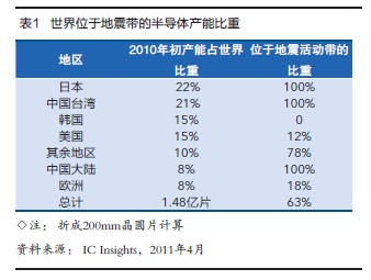
Since Japan’s 3.11 earthquake had caused production disruptions in 15 wafer fabs and caused negative impact on the semiconductor industry, ICInsights recently published a related report. According to its official juice, 63% of the world's semiconductor manufacturing capacity is located in the seismic activity zone, and the foundry production capacity is more than 90%. In particular, TSMC and UMC, two of the world’s top wafer foundries in Taiwan, are once In the event of an earthquake or hurricane disaster, it will have a huge impact on the overall electronics industry supply chain (see Table 1).
The 450mm wafer will be launched soon. Since 1980, the semiconductor industry has adopted l00mm wafers for production. The first generation is about every 5 years. In 1985, 150mm production was adopted; in l990, 200mm production was adopted; in 1995, 300mm production was used. Since it has been more than 15 years since 300mm, it has not yet gone to 450mm wafers of a new generation. The time can be described as long. Although there have been many discussions in recent years, no specific plans have been observed.
The reason for this is mainly the lack of driving force for the demand for breakthrough new products. It is said that the huge investment in 300mm wafer lines has not yet been fully recovered by manufacturers, thus lacking the economic strength to invest in new-generation processes. In addition, the development of a new generation of technology is not like the repetition of previous generations of processes, but requires that manufacturers of manufacturing equipment have comprehensive development capabilities, including process development, material preparation, software development, factory automation, etc., huge capital and expertise Not easy. Currently, even the world's largest equipment manufacturing companies like Applied Materials and Tokyo Electron are not able to independently complete such development in terms of resources.
In May 2008, when Intel, Samsung, and TSMC jointly announced the implementation of the 450mm production line, the industry shook. The economic storm can then be met, and the market is in a downturn. Until recently, people saw the movement of the promoters, especially Intel and TSMC, and published a more specific roadmap for development. TSMC plans to complete a prototype production line from 2013 to 2014 and mass production from 2015 to 2016. It plans to begin production on a 450mm wafer using 20nm process technology in the third quarter of 2012. Intel announced in February that it will invest more than US$5 billion to build a No. 42 plant in Arizona, use a process below l4nm, and build it in 2013. It is said that it will be the world’s most advanced factory.
TSMC’s technical forum held in San Jose, United States, on April 5, disclosed the company’s 450mm wafer production plan in detail. Taiwan Semiconductor Manufacturing Co., Ltd. will make every effort to advance to the 450mm era. One of its goals is to reduce costs. The other is to strive for a step ahead of the competition. The 450mm production line needs to invest about 10 billion U.S. dollars, of which the equipment cost is particularly high, but its productivity can be increased by 1.8 times than the 300mm production line, and the number of factories can be reduced to avoid the difficulty of finding a large number of outstanding engineering and technical personnel. The demand for personnel will be reduced in the next 10 years. people. It is reported that TSMC will first establish a prototype line at its No. 12 plant in Hsinchu, and it is expected to be put into operation from 2013 to 2014, and then it will be transferred to No. 15 plant in Taichung for mass production. It is planned to be completed from 2015 to 2016. Initially, 20nm process was used, and the future will be shifted to 14nm process.
When will Moore's Law come to the end?
The theory that Moore's Law has always been a standard in the semiconductor industry has long existed. iSuppli Company claimed in 2009 that Moore's Law will expire in 2014 and has caused heated discussions. When TSMC Chairman Zhang Zhongmou, known as the father of Taiwan's IC, attended the "Global Technology Summit" in late April this year, he said that Moore's Law will reach its limit in about 6 to 8 years. He said that Moore's Law has entered the new generation every two years on average and that there is not much room for micro IC development in the future. On the other hand, there is still space for development in the circuit board. It is necessary to develop new applications such as low power consumption in the future.
The difficulty of the development of micro-technologies is increasing day by day, from the 90-nm process in 2003, the 65-nm process in 2005, the 45-nm process in 2007 to the 32-nm in 2009, and it is a two-year generation. The interval between technological innovations after 2010 will be extended and is expected to slow from 22nm in 2011-2012, 15nm in 2014-2015, to 11nm in 2017-2018, and it will slow down to 2.5-3 generations.
In addition to the so-called "MoreMoore" method that continues to follow the traditional miniaturization path, the industry has also proposed a so-called "Morethan Moore" development path. It includes improving integration through 3D, and integrating analog circuits, power devices, sensors, biochips, and passive components into a single package, called SIP (System In Package). In addition, “Beyond CMOS†is another way proposed by the industry, that is, new devices that use different principles from the existing MOS transistors, including atoms, quantum, light, spintronics, etc. , and will become the basic technology of the 20th century.
In short, the future of integrated circuits will embark on a diversified development path. "Morethan Moore" and "BeyondCMOS" will become the driving force behind the development of "MoreMoore" technology. In addition, the use of compound semiconductors (Ge and III-V semiconductors) is also worthy of attention, and the industry has said that "there are materials for the world".
The next decade of agitated
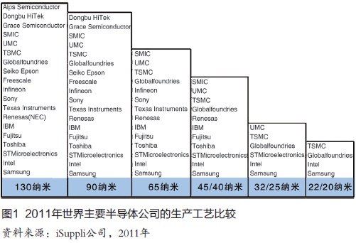
In any case, the road to miniaturization will continue. The current 32nm process has become mainstream technology. This year the world's major semiconductor manufacturers such as Intel, TSMC, GlobalF, Samsung and other companies will soon step into the 22nm generation of new technologies, but a comprehensive overview of the world's semiconductor industry production The company, from below 130nm, has a total of six generations of production processes coexisting in the world (Figure 1). It is expected that 22nm will become the mainstream production technology next year.
In addition, there is also a reference that micro-technology under the traction of NANDflash will continue to adopt new methods and the pace of progress will also accelerate, exceeding the prediction of ITRS (International Semiconductor Technology Roadmap), 1Xnm technology is about to become a success this year. 9nm technology has also been successfully developed in the laboratory. According to the ITRS roadmap, 2024 will enter the 5nm era. By then, the number of integrated transistors will exceed 25 billion cells per square centimeter. Of course, it must be renovating the original technology and applying new semiconductor materials.
In short, the world's semiconductor industry will flash and make room for the new decade, and it will be time for new ones. People must soberly realize this, and they will not miss the opportunity to advance. When the 22nm process was put into mass production from 2011 to 2012, existing MOS transistor structures and materials could be maintained. After the 15nm era from 2014 to 2015, new technologies for improving product performance must be developed.
Concluding remarks that things are always in development, life must have end. Moore's Law is to reduce the size of the process on semiconductor chips to improve its integration and reduce costs. This path cannot go any further and people have studied different methods to change the structure of M0S transistors, replace semiconductor materials, and 3D. The miniaturization of semiconductor technology continues to advance.
Ningbo Autrends International Trade Co.,Ltd. , https://www.mosvape.com