Mobile communication uses electromagnetic waves as the transmission carrier of signals for wireless communication. Therefore, its radio frequency circuit is in an important position on the mobile communication terminal. The performance of radio frequency is directly related to the signal receiving and transmitting capability and the communication capability between the terminal and the base station. The research on the design of RF circuits for mobile terminals and the development trend of RF devices used has become an important issue for terminal manufacturers.
In today's mobile terminal mainstream RF circuit, it mainly includes three parts, namely RF front-end circuit, transceiver circuit and frequency source circuit. Although the design ideas and materials and processes used in these three parts of the circuit are greatly different, the three are in the field of miniaturization and cost-effective development. Due to the nature of the materials used and the problem of transceiving, the three-part circuit is difficult to integrate. The three-part circuits develop independently in their respective fields and influence each other to jointly promote the evolution of RF circuits in communication terminals.
RF front-end circuits are moving toward miniaturization and interactive integrationSemiconductor manufacturers have been working on integrating various functions into large integrated circuits for many years, and terminal costs have been decreasing with increasing integration, bringing more and more benefits to consumers. In the RF circuit portion of the mobile communication terminal, many components are either integrated into the chip or disappear with the appearance of a direct digital up/down converter.
However, with the development of terminal circuits up to now, there are still two important devices that have not yet been integrated, namely RF front-end filters and RF power amplifiers. The build techniques used in both devices are not compatible with on-chip CMOS integration. Traditionally, filters have been constructed using ceramic or surface acoustic wave (SAW) technology, while RF power amplifiers have been constructed using gallium arsenide (GaAs) heterojunction bipolar transistors (HBT) or FET devices. Because these technologies are very different from the silicon or silicon germanium processes used in RF chips, amplifiers and filters have always been used as discrete devices, combined with large-scale integrated chips that now perform most of the RF functions of mobile phones.
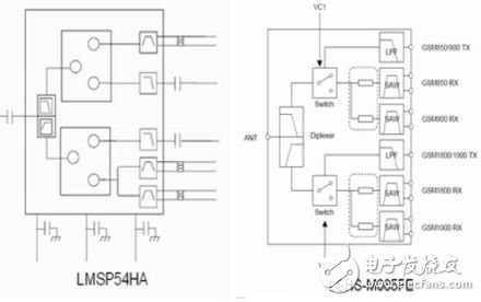
The mobile terminal RF front-end circuit mainly consists of three parts of the circuit: RF power amplifier, antenna switch or duplexer, front-end (image frequency) filter. Due to the problem of RF power amplifier and front-end filter transceiver isolation and process implementation, there is still a big problem in integrating them into a single chip. Antenna switch or duplexer manufacturers embed receive front-end filters on LTCC substrates, forming a popular RF front-end module (FEM) such as MURATA's LMSP54HA and Hitachi Metals' LSHS-M085FE due to its miniaturization And low cost advantage, has been widely used in a large number of GSM mobile terminals.

Figure 1: Block diagram of MURATA's LMSP54HA and Hitachi Metals' LSHS-M085FE.
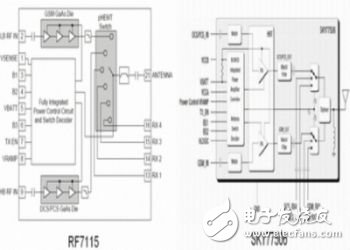
Amplifier manufacturers use the GaAs process to implement antenna switches or duplexers based on their power amplifier chips, which constitutes another popular RF front-end module, such as RFMD's RF7115 and SKYWORKS's SKY77506, due to its miniaturization and low The cost advantage is also widely used in the current GSM mobile terminal design. Antenna switch or duplexer manufacturers and RF power amplifier manufacturers are currently committed to the integrated development and research of the three. Therefore, the three-in-one RF front-end monolithic is an inevitable trend in the development of mobile terminal RF.

Figure 2: Power amplifier architecture diagram of the integrated antenna switch.
The development trend of transceivers is direct conversionThe development of RF transceiver chip has gone through three stages: the first stage, the super-heterodyne secondary frequency conversion fixed IF RF architecture stage; the second stage, the super-heterodyne secondary frequency conversion low-IF RF architecture stage; the third stage , using the direct conversion RF architecture stage;

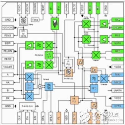
Figure 3: Transceiver single-chip solution using a superheterodyne secondary frequency conversion system architecture.
The first stage of the RF transceiver chip integrates the classic RF superheterodyne system architecture into a single chip. The IF filter with fixed frequency and bandwidth is used to select and filter the IF signal. The typical chip in this stage is INFINEON. The company's PMB6253 uses a 360MHz IF filter to perform up-and-down conversion processing and conversion of the transmitted and received signals.
The second stage of the RF transceiver chip adjusts the classical RF superheterodyne system architecture system, and greatly increases the frequency of the first local oscillator. After the first local oscillator is converted, the intermediate frequency signal with lower frequency is obtained. The intermediate frequency channel integrates a channel filter to complete the frequency selection and filtering of the intermediate frequency signal, and then obtains the radio frequency I and Q signals through the second local oscillator frequency conversion filtering, and sends the signal to the baseband chip for processing. The most important feature of the RF receiving and transmitting chip at this stage is that the external IF filter is eliminated, which effectively reduces the terminal cost. The low-IF RF transceiver chip is typically a MT612X chip such as Taiwan's MEDIA TEK.
The third stage of the RF transceiver chip uses a phase-locked loop. A VCO forms a local oscillator signal. After receiving and transmitting signals, the signal is directly converted into I and Q signals. Since the local oscillator signal is equal to the operating signal frequency, after the frequency conversion. The IF=0 can directly remove the IF filter.
Fiber Optic Field Connector,Fiber Optic Accessory,Optical Fiber Accessories,Optical Fiber Accessory
Huizhou Fibercan Industrial Co.Ltd , https://www.fibercannetworks.com