An embedded system is a "special computer system that is completely embedded inside a controlled device and designed for a specific application." For control, monitoring, or auxiliary equipment, machines, or equipment used in factory operations, the core is made up of one or several pre- Programped with a microprocessor or microcontroller that performs a few tasks. This article will introduce three application circuits based on embedded technology, namely motor drive controller, SOHO router circuit and embedded speech recognition circuit.
Motor drive controller
The DSP chip and the peripheral circuit are used to form the speed capture circuit. The motor drive controller adopts the micro control chip and the peripheral circuit to form the circuit of current sampling, overcurrent protection and pressure regulation. The CPLD is used to realize the logic change of the rotor position signal of the brushless DC motor. phase. The racing brake controller consists of an anti-skid controller and a motor drive controller. Both controllers are based on DSP chips. The anti-skid controller is mainly controlled by the slip rate, and outputs a given brake pressure. The DSP chip is used as the CPU, plus the racing wheel and the wheel speed signal conditioning circuit. The motor drive controller mainly adjusts the brake pressure and controls the motor current. It also uses the DSP chip as the CPU, plus the peripheral circuit motor current feedback conditioning circuit, overcurrent protection circuit, brake pressure conditioning circuit, and four sets of three-phase full bridge. The inverter circuit and the like constitute a motor drive controller.
Signal processing circuit: The anti-skid controller is mainly controlled by the slip rate to prevent the car from slipping. The pressure reference value is adjusted by the deviation of the slip rate to track the given slip rate. The anti-skid controller must have a conditioning circuit for the front wheel and brake wheel speed signals, mainly to obtain the feedback slip rate. The racing speed signal is replaced by a free-rolling front wheel speed signal. The speed sensor is installed on the front wheel and the brake wheel of the car. When the wheel rotates, the speed sensor generates an AC signal in the form of a sine wave. Each time the wheel rotates, the speed sensor emits a 50-cycle sinusoidal AC signal. The amplitude of the sinusoidal AC signal varies with the speed of the wheel. The signal is a sine wave signal with a bias voltage of 2.5V, a peak value of 0.3V, and a maximum signal amplitude of no more than 5V.
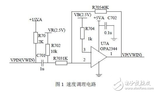
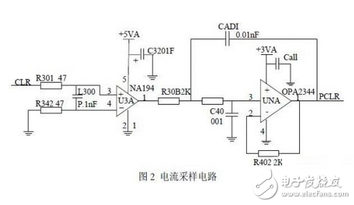
Current sampling and overcurrent protection circuit: The current of the brushless DC motor is detected by the resistance on the bus of the power drive circuit. The resistance above the busbar is connected in parallel by two 0.01Ω power resistors. The sampling circuit samples the current through the two parallel sampling resistors. The sampling resistor converts the current signal into a voltage signal, and the voltage signal is sent to the current monitoring chip for amplification. Then, it is filtered by the second-order active filter circuit composed of OPA2344, and finally the current feedback signal is directly sent to the A/D converter.
The hardware overcurrent protection circuit plays an important role in the normal operation of the system, mainly for the protection of the power device MOSFET and the motor. The system also has a software protection function. The overcurrent signal OVCURX is sent to the input pin of the DSP. When OVCUR is high, the DSP will generate a motor control rotation signal ENABLE to turn off the logic signal to stop the motor. The chip IR2130 itself has overcurrent protection.
SOHO router circuit
Utilize the Linux kernel to support IPMasquerade technology to achieve NAT conversion, and achieve multiple hosts to share access to the Internet. IPMasquerade works: the client sets the Linux machine that implements IPMasquerade as the default gateway. When the Linux machine of IPMasquerade receives the client's data packet, it rewrites it, replaces the source address with its own IP address, and the source port. Change the number to a new port number and record the process; when receiving the response packet, if the port number is the previously specified port number, then rewrite the packet and set its destination IP address. And the destination port number is replaced with the original recorded client IP address and port number, and then sent to the client.
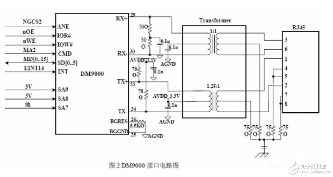
The S3C2410X microprocessor is connected to the FLASH and SDRAM through the system bus to form a storage system. After the system is powered on, the microprocessor reads the initialization program from the FLASH. The SDRAM provides temporary storage space for program operation and data processing and forwarding. The Ethernet control chip DM9000 is connected to the Internet via a single-port isolation transformer and RJ45 interface. The DM9000 is connected to the PORT4 port of the switching control chip RTL8305SC through MII (Independent Media Interface). The RTL8305SC is connected to a LAN hub, switch or computer via a 4-port isolation transformer and four RJ-45 interfaces for data exchange or microprocessor control and WAN. connection.
The DM9000 and S3C2410X and RJ45 interface circuits are shown in the figure. The pin INT of the DM9000E chip is connected to the external interrupt signal EINT14 of the S3C2410X chip. The S3C2410X chip select signal nGCS4 and the address line MA2 are respectively connected to the AEN pin and the CMD pin of the DM9000. SA6 to SA0 correspond to the address bus, while SA9 and SA8 pins are set to high level, SA7 pin is set low for chip select DM9000; 3C2410X nOE pin is connected to DM9000 read pin IOR#, nWE The pin is connected to the write pin IOW# of the DM9000, and the S3C2410X data line MD[0..15] is connected with the data line SD[0..15] of the DM9000 to realize data transmission. The RTL8305S port 5 is set to an MII interface connected to the Ethernet control chip DM9000RMII ​​interface. The RTL8305S is similar to the four-port isolation transformer and RJ45 interface.
Butt Connector,Lugs Insulated Female Connectors,Insulated Female Connectors,Non-Insulated Spade Terminals Wire Connector
Taixing Longyi Terminals Co.,Ltd. , https://www.longyicopperlugs.com