LTE is a long-term evolution of the UMTS (Universal Mobile Telecommunications System) technology standard developed by the 3GPP organization. The LTE system introduces key transmission technologies such as OFDM (Orthogonal Frequency Division Multiplexing) and MIMO (Multiple Input Multiple Output), which significantly increases spectrum efficiency and data transmission rate, and supports multiple bandwidth allocations: 1.4MHz, 3MHz, 5MHz, 10MHz, 15MHz and 20MHz, etc., and support the global mainstream 2G/3G frequency band and some new frequency bands, so the spectrum allocation is more flexible, system capacity and coverage are also significantly improved. The network architecture of the LTE system is flatter and simplistic, which reduces the complexity of network nodes and systems, thereby reducing system delay and reducing network deployment and maintenance costs. The LTE system supports interoperability with other 3GPP systems. To this end, this article introduces some of the LTE test circuit design.
TOP1 realizes voltage non-contact stability measurement circuit
Non-contact voltage measurement principle
The principle of non-contact voltage measurement is similar to that of a magnetometer that measures magnetic fields. It does not require a direct electrical connection. By capacitive coupling, the displacement current is used to measure the voltage on the surface of the object or free space. The sensor electrode is placed in the electric field, and a coupling capacitor is formed between the sensing electrode and the signal source, and a voltage dividing circuit is formed between the measuring system and the ground through the coupling capacitor signal source, as shown in FIG.
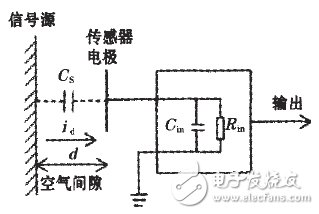
Figure 1 Schematic diagram of non-contact voltage measurement
When the coupling impedance is negligible compared to the system input impedance, the system is equivalent to a voltmeter with ideal characteristics to effectively measure the voltage signal. Therefore, in order to improve the sensitivity of the system, in the system design process, feedback technology should be used to improve the input resistance of the front-end sensor of the system and reduce the input capacitance. By measuring the magnitude of the two points in the air, the relationship between the voltage and the electric field can be derived.
Demystifying STM32 multi-channel voltage measurement circuit
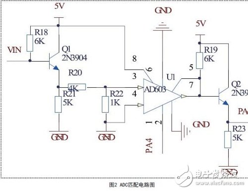
ADC control circuit module
In order to expand the measurement range and measurement accuracy, this design adds a matching circuit to the STM32's ADC. In the ADC control circuit, the input signal passes through the emitter voltage follower circuit and then passes through the voltage divider circuit to make the input signal meet the input requirements of AD603. It is then passed through the emitter voltage follower circuit and input to the ADC input. The control input of the AD603 uses the STM32 DAC to meet the gain requirements. The matching circuit is centered on AD603. The AD603 is a single-channel, low-noise, gain-variable linearly continuously adjustable gain amplifier. When the bandwidth is 90MHz, the gain varies from -10dB to +30dB. When the bandwidth is 9M, the range is 10~50dB. Short-circuit VOUT and FDBK, that is, broadband mode (90MHz wideband), and the gain of AD603 is set to -11.07dB. ~+31.07dB.AD603 is connected to pins 5 and 7. The adjustable range of single-chip AD603 is -10dB~30dB. The gain of AD603 is linear with the control voltage. The gain control terminal input voltage range is ±500mv, and the gain adjustment range is 40dB, when stepping 5dB, the control terminal voltage needs to increase:
The circuit diagram of the ADC matching circuit is shown in Figure 2.
SD card driver circuit
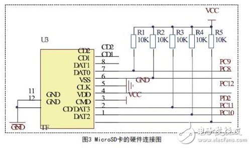
The SD card used in this design is MicroSD, also known as TF card. MicroSD card is a very small flash memory card, mainly used in mobile phones, but due to its small size and increasing storage capacity, it has been used in GPS devices, portable music players, digital cameras and some flashes. In the memory disk. Like the SD card, the MicroSD card has two operating time buses, SPI and SDIO. The SPI bus is simpler than the SDIO bus interface, but at a slower speed. We use the SDIO mode. The MicroSD card has 4 data lines in SDIO mode. In fact, MicroSD has 1 line mode and 4 line mode in SDIO mode, that is, 1 or 4 data lines respectively. Of course, the 4-wire mode is faster than the 1-wire mode, but the operation is more complicated. The 4-wire mode of SDIO is used in this design. The hardware connection diagram of the MicroSD card is shown in Figure 3.
Touch screen circuit
This design uses the touch screen to set the measured channel and display settings in addition to the button settings. The touch screen is controlled by the chip TSC2046, and its hardware connection diagram is shown in FIG. 4.
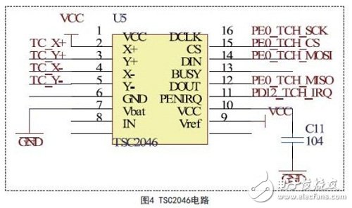
In FIG. 4, the TSC 2046 can acquire the point coordinates of the touch screen to determine the position of the touch and perform human-computer interaction. The STM32 MCU communicates with the TSC2046 via the SPI bus to obtain touch information. This design uses the touch screen to set the number of measurement channels and set the measurement speed.
The STM32 is superior in terms of speed and power consumption, and the STM32 is less expensive and has an advantage in cost. Suitable for controlling the design of electronic devices. A 12-bit ADC is used to meet certain measurement accuracy, and for higher measurement requirements, a higher accuracy ADC is required. However, the use of high-precision ADCs and DSP chips will greatly increase development costs. This design completes the functions of multi-channel voltage measurement, but it also needs to check its stability and reliability during use to make the design more perfect.
Global Electronic Measurement Technology and Market Leader - Keysight (formerly Agilent Electronic Measurement Division)
WDM (Wavelength Division Multiplexing) combines two or more optical carrier signals of different wavelengths (carrying various information) at the transmitting end through a multiplexer (also known as a multiplexer), and The technology of transmitting in the same optical fiber coupled to the optical line; at the receiving end, the optical carrier of various wavelengths is separated by a demultiplexer (also called a demultiplexer or demultiplexer), and then the optical carrier is The receiver performs further processing to restore the original signal. This technology of simultaneously transmitting two or more optical signals of different wavelengths in the same optical fiber is called wavelength division multiplexing.
Wavelength division multiplexing is a technology that uses multiple lasers to simultaneously send multiple lasers of different wavelengths on a single fiber. Each signal is transmitted in its unique color band after being modulated by data (text, voice, video, etc.). WDM can greatly increase the capacity of the existing fiber optic infrastructure of telephone companies and other operators. Manufacturers have introduced WDM systems, also called DWDM (Dense Wavelength Division Multiplexing) systems. DWDM can support the simultaneous transmission of more than 150 light waves of different wavelengths, and each light wave can reach a data transmission rate of up to 10Gb/s. This system can provide a data transmission rate of more than 1Tb/s on an optical cable that is thinner than a hair.
Optical communication is a way in which light carries signals for transmission. In the field of optical communications, people are accustomed to naming them by wavelength instead of frequency. Therefore, the so-called Wavelength Division Multiplexing (WDM) is essentially frequency division multiplexing. WDM is a system that carries multiple wavelengths (channels) on one optical fiber, and converts one optical fiber into multiple "virtual" fibers. Of course, each virtual fiber works independently on a different wavelength, which greatly improves the transmission capacity of the optical fiber. . Because of the economy and effectiveness of the WDM system technology, it has become the main means of expanding the capacity of the current optical fiber communication network. As a system concept, wavelength division multiplexing technology usually has three multiplexing methods, namely, wavelength division multiplexing with wavelengths of 1 310 nm and 1 550 nm, sparse wavelength division multiplexing (CWDM, Coarse Wavelength Division Multiplexing) and dense wave Division Multiplexing (DWDM, Dense Wavelength Division Multiplexing).
CWDM, DWDM, FWDM, LAN WDM, FBT WDM, AAWG WDM, Other WDM Related Equipment
Shenzhen GL-COM Technology CO.,LTD. , https://www.szglcom.com