Operational Amplifier Static Specifications
1. Input offset voltage (VIO): When the input voltage is zero, the output voltage is divided by the voltage gain, which is the offset voltage converted to the input. VIO is an indicator of the symmetry of the internal circuit of the op amp.
2. Input offset current IIO (input offset current): The difference between the base current of the differential pair of differential input stages at zero input is used to characterize the degree of asymmetry of the differential input current.
3. Input bias current (IB): The average of the two input bias currents of the op amp, which is used to measure the input current of the differential amplifier to the tube.
4. Input offset voltage temperature drift: In the specified operating temperature range, the input offset voltage changes with the temperature and the temperature change ratio.
5. Input offset current temperature drift: In the specified operating temperature range, the input offset current changes with the temperature and the temperature change ratio.
6. Maximum differential mode input voltage (maximum differential mode input voltage): The maximum differential mode input voltage that the two input terminals of the op amp can withstand. When this voltage is exceeded, the differential pipe will appear reverse breakdown.
7. Maximum common mode input voltage: The allowable range of the common-mode input voltage under the normal operational conditions of the operational amplifier. When the common-mode voltage exceeds this value, the input differential pair becomes saturated and the amplifier loses common-mode rejection.
Operational Amplifier Dynamic Specifications
1. Open loop voltage gain (open loop voltage gain): The ratio of the output voltage to the input voltage when the op amp is placed under no external feedback.
2. Input resistance: The input resistance of the op amp when a differential mode signal is input.
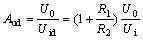
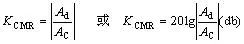
3. Common mode rejection ratio: The same as the definition in the differential amplifier circuit, which is the ratio of the differential-mode voltage gain to the common-mode voltage gain, commonly expressed in decibels. KCMR=20lg(Avd/Avc) (dB)
4.-3dB bandwidth (-3dB band width): The bandwidth defined by the differential mode voltage amplification of the op amp drops 3dB at high frequencies.
5. Unit gain band width (BW?G): The frequency corresponding to a drop to 1 is defined as unity gain bandwidth.
6. Slew Rate: It reflects the ability of an op amp to respond to rapidly changing input signals.
7 equivalent input noise voltage Vn (equivalent input noise voltage): When the input is short-circuited, the noise voltage at the output is converted to the input value. This value often corresponds to a certain frequency band.
Integrated operational amplifier indicator test
The integrated operational amplifier is a kind of linear integrated circuit. Like other semiconductor devices, it uses some performance indicators to measure its quality. In order to use the integrated operational amplifier correctly, it is necessary to understand its main parameters. The indicators of integrated op amp components are usually tested by special instruments. Here is a simple test method.
The integrated operational amplifier model used in this experiment is μA741 (or F007). The pinout is shown in Figure 7-1. It is an 8-pin dual in-line module. Pins 2 and 3 are the inverting and non-inverting inputs. 6 feet is the output end, 7 feet and 4 feet are the positive and negative power end, 1 foot and 5 feet are the misalignment zeroing end, 15 feet can access a potentiometer of several tens of K ohms and connect the sliding contact To the negative power terminal. 8 feet are empty.
1, μA741 main indicators test
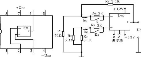
Figure 7-1 μA741 pin diagram Figure 7-2 U0S, I0S test circuit
1) Input offset voltage U0S
Ideal op amp components, when the input signal is zero, its output is also zero. However, even the best integrated components, because of the incomplete symmetry of the internal differential input stage parameters of the op amp, the output voltage is often not zero. This non-zero output at zero input is called the offset of the integrated op amp.
The input offset voltage U0S is the value at which the voltage present at the output is converted to the non-inverting input when the input signal is zero.
The offset voltage test circuit is shown in Figure 7-2. Close the switches K1 and K2 to short the resistor RB. Measure the output voltage U01 at this moment as the output offset voltage, then input the offset voltage.
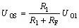
The actual measured U01 may be positive or negative, typically 1 to 5 mV, and for a high-quality op amp U0S is less than 1 mV.
Should pay attention to the test: a, will open the amplifier zero.
b. The parameters R1 and R2, R3 and RF are required to be strictly symmetrical.
2) Input offset current I0S
The input offset current I0S is the difference between the base bias currents of the two input terminals of the op amp when the input signal is zero.

The magnitude of the input offset current reflects the mismatch of the two transistors β in the op amp's internal differential input stage. Since the values ​​of IB1 and IB2 are already very small (micro-ampere level), their difference is usually not directly measured. The test circuit is shown in Figure 7-2. The test is performed in two steps.
a. Close the switches K1 and K2. Under the low input resistance, measure the output voltage U01. As mentioned above, this is the output voltage caused by the input offset voltage U0S.
b, disconnect K1 and K2, two input resistors RB access, because RB resistance is larger, the difference of the input current flowing through them, will become the input voltage difference, therefore, will also affect the size of the output voltage, It can be seen that the output voltage U02 when the two resistors RB are connected is detected. If the influence of the input offset voltage U0S is deducted therefrom, the input offset current I0S is
In general, I0S is about tens to several hundred nA (10-9A), high quality op amp IOS is lower than 1nA.
Should pay attention to the test: a, will open the operational amplifier zero.
b. The two input resistors RB must be precisely matched.
3) Open-loop differential mode Aud
The dc differential mode amplification when the integrated carrier is placed in the absence of external feedback is called the open loop differential mode voltage amplification, denoted by Aud. It is defined as the ratio of the signal voltage Uid applied between the open-loop output voltage U0 and the two differential inputs.

According to the definition, Aud should be the DC amplification factor when the signal frequency is zero, but for the convenience of testing, low-frequency (several tens of Hertz or less) sinusoidal AC signals are usually used for measurement. Because the open-loop voltage of the integrated operational amplifier has a high amplification factor and it is difficult to directly measure, a closed-loop measurement method is generally used. Aud's test methods are many and now use AC and DC simultaneous closed-loop test methods, as shown in Figure 7-3.
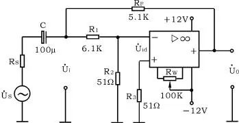
Figure 7-3 Aud test circuit
On the one hand, the op amp to be tested completes DC closed loop through RF, R1 and R2 to suppress the output voltage drift. On the other hand, it realizes AC closed loop through RF and RS. The additional signal uS is divided by R1 and R2 to make uid small enough to guarantee The op amp operates in the linear region. The non-inverting input resistor R3 should be matched with the inverting input resistor R2 to reduce the influence of the input bias current. The capacitor C is a DC blocking capacitor. The open loop voltage amplification of the op amp under test is
Generally, the low-gain op amp Aud is about 60 to 70 db, the mid-gain op amp is about 80 db, and the high gain is above 100 db, which can reach 120 to 140 db.
It should be noted in the test: a. Before the test, the circuit should first be damped and zeroed.
b. The op amp to be tested must work in the linear region.
c, the input signal frequency should be low, generally 50 ~ 100HZ, the output signal amplitude should be small, and no obvious distortion.
4) Common mode rejection ratio CMRR
The ratio of the differential mode voltage amplification Ad of the integrated operational amplifier to the common mode voltage amplification ratio AC is called the common mode rejection ratio.
The common mode rejection ratio is a very important parameter in the application. The ideal op amp has zero output for the input common mode signal, but in the actual integrated op amp, the output cannot have no common mode signal components. The smaller the common-mode signal, the better the symmetry of the circuit, that is, the stronger the ability of the op amp to suppress common-mode interference signals, that is, the larger the CMRR. The test circuit of CMRR is shown in Figure 7-4.
The differential mode voltage amplification of the integrated op amp in a closed-loop state is

When accessing the common-mode input signal Uic, U0C is measured, then the common-mode voltage amplification is

Common mode rejection ratio
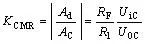
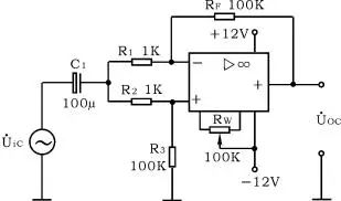
Figure 7-4 CMRR test circuit
The test should pay attention to: a, damper and zero
b. Strictly symmetrical resistance between R1 and R2, R3 and RF
c. The amplitude of the input signal Uic must be less than the maximum common-mode input voltage range of the integrated op amp Uicm
5) Common Mode Input Voltage Range Uicm
The maximum common-mode voltage that the integrated op amp can withstand is called the common-mode input voltage range. Outside this range, the CMRR of the op amp will be greatly degraded, the output waveform will be distorted, and some op amps will also appear “self-locking†and permanent. The damage.
The Uicm test circuit is shown in Figure 7-5.
The op amp under test was connected in the form of a voltage follower. The output was connected to an oscilloscope and the maximum undistorted output waveform was observed to determine the Uicm value.
6) Output voltage maximum dynamic range UOPP
The dynamic range of the integrated op amp is related to the supply voltage, external load, and signal source frequency. The test circuit is shown in Figure 7-6.
Change the uS amplitude and observe the starting moment of the u0 cut-off distortion, so as to determine the undistorted range of u0. This is the peak-to-peak value of the voltage UOPP that can be output at a certain supply voltage.
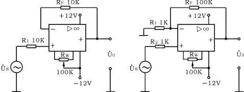
Figure 7-5 Uicm test circuit Figure 7-6 UOPP test circuit
2. Some issues that should be considered when integrating the shipments into use
1) The input signal can be selected to be AC ​​or DC. However, when selecting the frequency and amplitude of the signal, the frequency response characteristics and output amplitude of the operational amplifier should be considered.
2) Zero adjustment. In order to improve the operation accuracy, the DC output potential should be zeroed first before the operation, that is, when the input is zero, the output is also zero. When the op amp has an external zero terminal, it can be connected to the zero potentiometer RW according to the component requirements. When it is zeroed, the input terminal is grounded, the zero terminal is connected to the potentiometer RW, and the output voltage U0 is measured with a DC voltmeter. Adjust RW so that U0 is zero (that is, the offset voltage is zero). If the op amp has no zero terminal, if it is zero, it can be adjusted according to the circuit shown in Figure 7-7.
If an op amp cannot be zeroed, there are roughly the following reasons: 1 The component is normal and the wiring is wrong. 2 The components are normal, but the negative feedback is not strong enough (RF/R1 is too large). To do this, short the RF and observe if it can be zeroed. 3 The component is normal, but because it allows the common-mode input voltage to be too low, self-locking may occur and it cannot be zeroed. For this reason, the power supply can be disconnected and then turned back on. This can be the case if it returns to normal. 4 The components are normal, but the circuit has self-excitation and should be dampened. 5 The internal damage of the component should be replaced with a good one.
(a) (b)
Figure 7-7 Zeroing circuit
3) Vibration suppression. When an integrated op amp is self-excited, it shows that even if the input signal is zero, there will be an output, so that a variety of computing functions can not be achieved, in serious cases will damage the device. In the experiment, an oscilloscope can be used to monitor the output waveform. In order to eliminate the self-excitation of the op amp, the following measures are often used:
1 If the op amp has phase compensation terminals, an external RC compensation circuit can be used. The product manual provides compensation circuit and component parameters. 2 Circuit layout, elements, and device layout should minimize the distributed capacitance. 3 Connect tens of μF electrolytic capacitors and 0.01-0.1μF ceramic capacitors in parallel between the positive and negative power supply lines and the ground to reduce the influence of the power supply leads.
What is PSRR
PSRR is the abbreviation of Power Supply Rejection Ratio. The Chinese meaning is “power supply rejection ratioâ€. That is, PSRR represents the ratio of the two voltage gains obtained when the input and the power supply are treated as two separate sources. The basic calculation formula is:

PSRR is measured in decibels (dB) using a logarithmic ratio where V1 is the change in the input voltage and V2 is the change in the output voltage.
From the above formula, it can be seen that the factors affecting the output signal are influenced by the power supply in addition to the circuit itself. PSRR is a quantity used to describe the output signal affected by the power supply. The larger PSRR is, the smaller the output signal is affected by the power supply. The result of this equation is generally zero. If you see a power supply trademark with a positive PSRR value, don't be surprised, it's just because they are using V2 versus V1 instead of V1 versus V2. As long as you take the absolute value of PSRR, you can avoid all the confusion. Designers all hope that the higher the absolute value of the PSRR, the better, because the higher the absolute value of the PSRR, the lower the noise/wave on the output. For example, an absolute value of 80 dB PSRR (output ripple is 10,000 times smaller than input ripple) is better than an absolute value of 20 dB (output ripple is 10 times smaller than input ripple).
It can also be concluded that the output voltage Vout is a function of Vin and the supply voltage VCC. If the input signal Vin changes by ⊿Vin, the amount of change 输出Vout of the output signal is the voltage gain Av from the input to the output multiplied by the amount of change 输入Vin of the input voltage. If the power supply voltage change ⊿VCC is regarded as a very small signal, the output voltage change ⊿Vout due to the power supply voltage change is the voltage gain from the power supply voltage to the output Avo multiplied by the power supply voltage variation ⊿VCC.
Unstable power supply voltage is bound to affect the waveform of the output signal, and the magnitude of the effect depends on the PSRR. Therefore, it is necessary to focus on the decoupling design of the op amps and the design of the power supply (usually the LDO linear power supply is usually used to power the op amp). PSRR is obtained with unit closed-loop gain, so the output change caused by negative feedback applications needs to be multiplied by the closed-loop gain.
In general, PSRR has three specific parameters: +PSRR, -PSRR, and +/-PSRR. It represents the transmission or influence value that is introduced at the differential input of the op amp from the low-frequency change of the opposite-side low frequency of one power supply or two power supplies. As analyzed above, a power change of ⊿Vps = 1V at the input of the PRSS = "80dB" op amp results in a change in ⊿Vdi = 100uV (PSRR = 20log ⊿ Vps/⊿Vdi). Then the output voltage of the op amp changes: ⊿Vo=⊿Vdi (1+Rf/Ri); Rf--feedback resistor, Ri-- input resistance.
Absolute Linear Encoders,Custom Absolute Encoder,Rotary Encoder Magnetic,Miniature Absolute Encoder
Yuheng Optics Co., Ltd.(Changchun) , https://www.yhenoptics.com