one. TTL
The main type of TTL integrated circuits is the transistor-transistor logic gate. Most of the TTL uses a 5V power supply.
1. Output high level Uoh and output low level Uol Uoh ≥ 2.4V, Uol ≤ 0.4V
2. Input high level and input low level Uih ≥ 2.0V, Uil ≤ 0.8V two. CMOS
CMOS circuit is a voltage control device, the input resistance is very large, and it is very sensitive to the interference signal. Therefore, the unused input should not be opened, connected to the ground or the power supply. The advantage of the CMOS circuit is that the noise margin is wide and the static power consumption is small. .
1. Output high level Uoh and output low level Uol Uoh≈VCC, Uol≈GND
2. Input high level Uoh and input low level Uol Uih ≥ 0.7VCC, Uil ≤ 0.2VCC (VCC is the power supply voltage, GND is the ground)
As can be seen from the above:
In the same 5V power supply voltage, the COMS circuit can directly drive TTL, because the CMOS output is higher than 2.0V, the output low level is less than 0.8V; and the TTL circuit can not directly drive the CMOS circuit, the TTL output is high. If it is greater than 2.4V, if it falls between 2.4V and 3.5V, the CMOS circuit can't detect the high level, and the low level is less than 0.4V. Therefore, the pull resistor should be added when the TTL circuit drives the COMS circuit. If there are different voltage sources, you can also judge by the above method.
If a 3.3V COMS circuit is used in the circuit to drive a 5V CMOS circuit, such as a 3.3V microcontroller to drive the 74HC, there are several ways to solve this problem. The simplest is to directly convert the 74HC to 74HCT (74 series input). Output the chip shown below, because 3.3V CMOS can directly drive the 5V TTL circuit; or add the voltage conversion chip; there is the I / O port of the microcontroller is set to open drain, and then add the pull resistor to 5V, In this case, the size of the resistor should be adjusted according to the actual situation to ensure the rising edge time of the signal . Introduction to the 74 series
The 74 series can be said to be the most common chip we usually touch. There are many types in the 74 series, and the ones we usually use the most are the following: 74LS, 74HC, 74HCT, these three series are at the level. The differences are as follows:
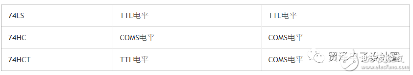
TTL and CMOS levels
1, TTL level (what is TTL level):
Output high level>2.4V, output low level=2.0V, input low level Vih, input low level Vih > Vt > Vil > Vol
6: Ioh: Load current when the logic gate output is high (to draw current). 7: Iol: Load current when the logic gate output is low (for sink current). 8: Iih: logic gate input is high Normal current (for sinking current). 9: Iil: Current when the logic gate input is low (current is drawn).
The gate output pole is directly connected to the integrated circuit as the output terminal. This type of gate is called an open gate. The open TTL, CMOS, and ECL gates are called open collector (OC) and open drain, respectively. (OD), open emitter (OE), should be used to check whether the pull-up resistor (OC, OD gate) or pull-down resistor (OE gate) is connected, and whether the resistance is suitable. For open collector (OC) gates, The pull-up resistor value RL should satisfy the following conditions:
(1): RL < (VCC-Voh)/(n*Ioh+m*Iih)(2): RL > (VCC-Vol)/(Iol+m*Iil)
Where n: the number of open gates with lines and m: the number of inputs driven.
10: Commonly used logic levels
· Logic level: TTL, CMOS, LVTTL, ECL, PECL, GTL; RS232, RS422, LVDS, etc.
· Logic levels of TTL and CMOS can be divided into four categories according to typical voltage: 5V series (5V TTL and 5V CMOS), 3.3V series, 2.5V series and 1.8V series.
· 5V TTL and 5V CMOS logic levels are common logic levels.
The logic level of 3.3V and below is called the low voltage logic level, and the LVTTL level is commonly used.
· Low voltage logic levels are also available in 2.5V and 1.8V.
· ECL/PECL and LVDS are differential input and output.
RS-422/485 and RS-232 are serial interface standards, RS-422/485 is differential input and output, RS-232 is single-ended input and output. OC gate, also known as open collector (open drain) and non- Gate circuit, Open Collector (Open Drain).
Why introduce OC gates?
In actual use, sometimes two or more NAND gate outputs are required to be connected to the same wire, and the data on the NAND gate (state level) is sent out by the same wire. Therefore, a need is needed. The new NAND gate circuit - OC gate to achieve "line and logic". OC gate is mainly used in three aspects:
1. Realize NAND logic, use level conversion, use as driver. Since the collector of the output tube of OC gate circuit is floating, use an external pull-up resistor Rp to the power supply VCC.OC gate to use pull-up resistor. The output level is high. In addition, in order to increase the driving capability of the output pin, the selection principle of the pull-up resistor value should be sufficiently large to reduce the power consumption and the current sinking capability of the chip; it should be small enough to ensure sufficient driving current. .2, line and logic, that is, the direct connection of two outputs (including more than two) can realize the logical function of "AND". In practical applications such as bus transmission, the output terminals of multiple gates need to be connected in parallel, and Generally, the TTL gate output terminals cannot be directly connected in parallel. Otherwise, the output transistors of these gates form a large short-circuit current (sink current) due to low impedance, and the device is burned out. On the hardware, an OC gate or a tri-state gate can be used. (ST gate) to achieve. Use OC gate to achieve line and should also add a pull-up resistor at the output port. 3, three-state gate (ST gate) is mainly used in multiple gate output shared data bus, in order to avoid Multiple gate outputs simultaneously occupy data Line, only one of the enable signals (EN) of these gates is allowed to be active (such as high level), because the output of the tri-state gate is a push-pull low-impedance output, and no pull-up (load) is required. Resistance, so the switching speed is faster than the OC gate, commonly used three-state gate as an output buffer. What is OC, OD?
Open collector gate (collector open OC or open drain OD)
Open-Drain is the open-drain output, which is equivalent to the open-collector output, which is the open collector (OC) output in TTL. It is generally used for line or line and also for current drive. .
Open-Drain is for MOS tube, Open-Collector is for bipolar tube, there is no difference in usage. Open-drain circuit has the following characteristics:
a. Use the driving ability of the external circuit to reduce the internal driving of the IC. Or drive the load higher than the power supply voltage of the chip. b. Connect multiple Pins of open-drain output to one line. Through a pull-up resistor, In the case of no adding any device, the relationship with "logic" is formed. This is also the principle that I2C, SMBus and other buses judge the bus occupancy state. If the totem output must be connected to the pull-up resistor. When the capacitive load is connected, the falling delay is the chip. The internal transistor is active drive, and the speed is fast; the rising delay is a passive external resistor, and the speed is slow. If the speed is high, the resistance selection is small, the power consumption will be large. Therefore, the load resistance should be selected with both power consumption and speed. .c. The voltage of the pull-up power supply can be changed to change the transmission level. For example, a pull-up resistor can be used to provide a TTL/CMOS level output. etc. The open-drain pin is not connected to an external pull-up resistor. Output low level. In general, open drain is used to connect different levels of devices, matching levels.
The normal CMOS output stage is the upper and lower tubes. The removal of the upper tube is OPEN-DRAIN. The main purpose of this output is two: level shifting and line and.
Since the drain is open, the post-stage circuit must be connected to a pull-up resistor. The supply voltage of the pull-up resistor determines the output level. This allows you to convert at any level.
The line and function are mainly used when there are multiple circuits to pull down the same signal. If the circuit does not want to pull low, it outputs a high level because the tube above OPEN-DRAIN is removed, and the high level is externally connected. The pull-up resistor is implemented. (And the normal CMOS output stage, if one output is high and the other is low, it is equal to the power supply short.)
OPEN-DRAIN provides a flexible output mode, but it also has its weakness, which is the delay of the rising edge. Because the rising edge charges the load through an external pull-up passive resistor, the delay is small when the resistor is selected, but The power consumption is large; on the contrary, the delay is large and the power consumption is small. Therefore, if there is a requirement for the delay, it is recommended to use the falling edge output.
Insulated Terminals,Terminals,High-quality insulated terminals
Taixing Longyi Terminals Co.,Ltd. , https://www.txlyterminals.com