When designing an I/O circuit, there are two important places: the functional subsystem and the "quiet area." The following will be explained separately.
Functional subsystemEach I/O should be treated as a different block of the PCB because they each have unique features and applications. In order to avoid RF coupling between subsystems, it must be split. A functional subsystem contains a bunch of components, as well as associated support circuitry. Components and components are in close proximity to each other, which shortens the length of routing and improves the performance of each functional block. Every hardware and PCB engineer will usually try to group components together, but sometimes it doesn't work for a variety of reasons. In the layout, the I/O subsystem is handled differently than other PCB blocks, which are usually achieved via wire cuts.
Wiring cut enhances the signal quality and the integrity of the function because it prevents the generation of high-frequency transmitters such as backplane interconnects, video devices, data interfaces, Ethernet controllers, SCSI devices, CPUs, and broken serials. Or parallel, video, audio, asynchronous/synchronous communication ports, floppy disk controllers, front-end displays, regional and wide area network controllers...etc. Each I/O subsystem must be treated like a different PCB.
Quiet areaThe "quiet area" is the area that is isolated from the digital circuit, analog circuit, power supply, and ground plane. This isolation can avoid noise sources in other PCB blocks and damage sensitive circuitry. For example: Power plane noise from digital blocks, infiltrated into analog devices (analog blocks), audio devices (audio blocks), I/O filters, interconnect circuits... . The power supply pins, as shown in Figure 1.
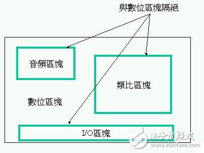
Figure 1: Quiet area
Each I/O port (or block) must have a cut (quiet) ground or power plane. Low frequency I/O ports can be bypassed using high frequency capacitors (usually 470 pF to 1,000 pF) close to the connector.
The routing on the PCB must be controlled so that re-coupled RF current does not flow into the shield of the cable. A clean (quiet) ground must be at the point where all cables leave the system. The power and ground planes must be treated equally because both planes are possible paths for RF return current. The RF return current from the switching device to the I/O control circuit brings high frequency wide, switched RF noise to the I/O cables and interconnects.
In order to create a quiet area, you must split it. This quiet area may be:
1. 100% is isolated from the I/O signal, and the signal must pass through an isolated transformer whether entering or leaving the signal.
2. The data line must be filtered.
3. Filter through a high impedance common mode inductor or use a ferrite bead-on-lead protection.
The main purpose of segmentation is to separate dirty power supplies, ground planes, and other functional areas from clean or quiet areas.
Isolation and segmentationIsolation and segmentation refers to the separation of components, circuits, and power planes from other functional devices, areas, and subsystems. If radio frequency currents are allowed to be transmitted to other parts of the circuit board by radiation or conductance, this will not only cause EMI problems, but will also destroy the normal functions.
Isolation is to make all planes of a certain area on a circuit board without copper wire. The area where no copper wire exists is called "moat". The width of the area where no copper wire is present is usually 0.05 inch. In other words, an isolated area is an "island" on a circuit board, similar to a castle with a castle. Only those traces that need to work or interconnect with it can be connected to this isolated area. For signals and traces, “ditching†is an isolated zone. These signals and traces are independent of the interface of isolated areas or isolated areas.
There are two ways to connect traces, power, and ground planes to this "island." The first method is to use an isolated transformer, optical isolator, or common-mode data line filter to span the "ditch." The second method is to use a "bridge" on the "ditch". Isolation is also used in applications where high-frequency wide components are separated from low-frequency circuits; in addition, it is also used to maintain the I/O interface at low EMI bandwidth—that is, from the I/O interconnect circuit. RF spectrum size.
Method One: Isolation
This is achieved using an isolated transformer or optical isolator. An I/O area must be 100% isolated from the rest of the PCB. Only on the metal I/O connector, the RF signal will be combined with the ground plane of the chassis, and only grounded through a low impedance, high quality protection path. In addition, the ground plane of the chassis must be separated from this isolation area. Sometimes due to design requirements, a bypass capacitor must be used between the shield ground (or braid isolation) of the I/O cable and the chassis ground instead of a direct connection. A shielded ground or drain wire refers to an individual pin or line on the interface connector, and the internal leakage line of the external I/O cable is connected to its mylar foil shield. The mylar shield is also located inside the cable. In any case, you cannot use a pigtail wire to connect the outer layer of the BNC connector to the ground plane of the chassis or any grounding system. The measurement results show that two RF signals operating in the same range of 15 to 200 MHz are transmitted in the tail wire and the other is transmitted in the cable shield that makes a 360-degree connection to the outer layer of the BNC connector. 40 to 50dB error. This can not only reduce RF radiation, but also improve the immunity of ESD, because when the ESD occurs, its wire inductance is relatively small. For most applications, it is best to connect the cable shield to the outer layer of the BNC connector and make a 360-degree connection. This connector backshell is finally combined with a bulkhead panel that contains a metal face that can be connected to the ground plane of the chassis.
Common-mode data line filters can be combined with isolated transformers to extend the effect of common-mode rejecTIon. Common-mode data line filters (usually spiral-shaped) can be used in analog and digital signal applications. These filters minimize common-mode RF currents transmitted from the signal line to the I/O block or cable. If power and grounding are required in the isolated area, for example, a keyboard or mouse requires +5 VDC, a powder core wire can be used to cross the “ditch†to form a power supply trace and a return trace. The width of the return trace is three times the power trace. Using a common-mode toroid to connect power and ground is also a suitable method. If necessary, the secondary short-circuit fuses (safe for the protection of the product) can be located on either side of the iron powder core. Sometimes, decoupling capacitors must be used to remove the digital noise in the filtered I/O supply. One end of this additional decoupling capacitor can be located on the filter side (output side) of the iron powder core and the other end on an isolated ground plane. The power filter assembly can span the "ditch" on the outermost edge of the board. The power and ground traces must be adjacent to each other to reduce the size of the RF ground loop. If they are located on either side of the “ditch†and facing each other, a RF ground loop will be generated between them. The example is shown in Figure 2.
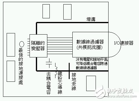
Figure II: Using Segregation Method to Cross the "Ditch"
Method two: Bridge
This method uses a "bridge circuit" between a control block and an isolated area. The location of the bridge is where the "ditch" cannot be circulated. Through it, signal lines, power and ground lines can all pass through the "ditch". As shown in Figure 3. Any route that is not related to the I/O line passes through the "ditch", it may cause RF radiation and ESD problems. The resulting RF loop current is shown in Figure 4. Radio frequency currents must be returned along their trace path "image". Common mode noise can occur between two different areas. The difference from the method is that the power and ground planes are directly connected between these two different areas. Therefore, this method forms a segmentation.
The advantage of using the bridging method is similar to the advantage of the castle being surrounded by "city." Only those who have "passports" can pass this "bridge." Because the RF return current must be returned along its trace path, magnetic flux can be minimized. This image return path is unique, and only one return path exists--that is, "this bridge."
Sometimes, only the power plane is isolated, and the ground plane can be completely connected through “this bridgeâ€. This technique is often used on circuits that need to be commonly grounded or individually filtered, and they all require a stable power supply. In this case, iron powder core wire is usually used to cross the "trench", but only the filtered power supply can do this. This powdered iron core must be located in the bridge area and must not cross the "ditch". If an analog or digital power supply is not required in the isolated area, this unused power plane can again be defined as a second 0V (ground) plane and referenced to the main ground plane. When using a "split plane", it must be ensured that the traces crossing the "bridge" do indeed follow a 0V reference (ground) plane, and not along the split power plane.
When using the bridging method, if the chassis and system level design provide mulTIpoint ground, it is best to connect both ends of the “bridge†to the chassis or frame together. Grounding the access port and the "bridge" can perform the following two functions:
1. It can remove high-frequency common-mode RF components (ground noise voltage) in the power supply network to prevent it from being coupled into the segmented region.
2. It can remove eddy currents that may be present in the chassis or in the card cage. In this way, the control of the ground loop can be improved.
A path with a lower impedance can be used as a ground plane for the RF current. Without it, the RF current can reach the ground plane of the chassis via other paths, such as the RF current in the I/O cable.
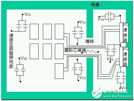
Photo 3: "Bridges" that span "ditches"
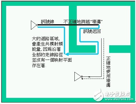
Figure 4: Examples of incorrect use of "trenches"
Grounding both ends of the "bridge" can also increase the immunity of ESD. If a high-energy pulse is injected into the I/O connector, this energy may go to the main control area and cause permanent damage. Therefore, this energy pulse must flow through a very small impedance path to the ground plane of the chassis. Another reason to ground both ends of the "bridge" is to remove the RF ground noise voltage due to the voltage difference between the divided area and the master area. If RF common-mode noise contains RF energy at high frequencies, decoupling capacitors must be used at each chassis ground to remove this RF energy (AC waveform). Figure 4 shows how the traces should be routed when using digital and analog segmentation. Because the switching noise of the digital power plane may be injected into the analog block, an isolation or filtering method must be used. All traces from the number to the analog block must go through the "bridge." For analog power supplies, an iron powder core wire must be used to span the "ditch". It may also require a voltage regulator. In general, "ditching" is 100% around the divided analog power supply area.
Some analog components need to connect analog ground to digital ground, but this must be done through a "bridge." As shown in Figure 5. There are many analog-digital and digital-analog devices that connect their analog ground (AGND) and digital ground (DGND) in the same package configuration. When the interior of a component is designed using this partitioning method, only one grounding connection (ie, sharing a grounding line) is required for analog and digital grounding during PCB layout. AGND and DGND need to be separated from each other by a "ditch" only when there is internal separation between AGND and DGND. When conducting PCB layout, engineers must ask the component supplier in advance how to properly isolate or connect AGND and DGND.
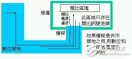
Figure 5: The concept of digital and analog segmentation
Incorrect use of mapping planeAlthough the mapping plane is useful, if it is used incorrectly, it will cause serious electromagnetic interference problems. An image plane must be able to be effective. All signal traces must be adjacent to a fixed plane and must not cross isolated copper areas. However, the use of some special routing winding technology is an exception. If a signal trace, or even a power trace (for example, a +12 V trace on a +5 V power plane) is wound in a fixed plane, the fixed plane will be cut into many small parts Copies. A design rule for returning a ground or RF signal to the loop has been established. This is the measurement of the RF return current between adjacent layers of the circuit board. The existence of this current represents that the mapping plane has not been used correctly. This type of RF loop is generated because the RF current cannot find a direct, low impedance return path within the signal trace.
Figure 6 illustrates the situation where the mapping plane is used incorrectly. These planes can no longer be a fixed 0 V reference point to remove common-mode RF currents. Due to the loss caused by the planar cutting, an RF electric field may eventually be generated. Vias on a mapping plane do not weaken the mapping capability of the plane, except for ground slots.
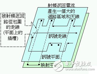
Figure 6: The alignment uses the mapping plane incorrectly
Another issue related to the discontinuity of the ground plane is the use of through-hole assemblies. Using too many piercing components on a power or ground plane will create the so-called "Swiss Cheese Syndrome." Due to too many holes, many holes overlap with each other, resulting in the reduction of copper blocks in the plane and the discontinuous areas become larger. This effect is shown in Figure 7. The return current on the mapping plane flows along the edges of the holes while the signal traces cross the discrete blocks in a straight path. As shown in Figure 7, the return current on the ground plane must bypass the slot or hole. As a result, the length of the trace must be increased to deliver the return current. Increasing the length of the trace will increase the inductance of the return trace. Because E = L(dI/dt), when the inductance value of the return path increases, the differential mode coupling effect between the signal trace and the RF current return path decreases, and the effect of flux cancellation (Fontal cancellaTIon) also decreases. . For holes that are not very large holes—there are still spaces between pins, and the best way to reduce the signal and return current is to reduce the inductance of the return path and the fixed plane.
If a signal trace walks along a hole area (discontinuous area), a fixed mapping plane (RF return path) will exist along all signal paths. On the right side of Figure 7, since there is no discontinuity in the ground plane, the length of the trace can be shortened. On the contrary, on the left side of Figure 7, if the length of the trace increases, the inductance value increases. When the length of the trace increases, it will cause energy reflection, destroy the integrity and proper function of the signal, and will also generate the RF current loop, just like an antenna.
In order to shorten the length of the traces and the signal traces must be routed through the slots or holes in the PCB, the “3-W rule†must be observed between the traces and the space near the holes: the spacing between the traces must be It is three times the width of a single trace; or, the spacing between two traces is twice the width of a single trace.
Figure 8 uses capacitors to enable RF return currents to traverse slots or "ditches." This capacitor provides an AC parallel circuit for the RF current so that the RF current can pass through the "ditch". It can improve performance by about 20dB. However, this method may cause a reactance displacement between the trace currents and their mapped currents, which will eventually weaken the effect of flux cancellation. Therefore, it is better to use the above isolation method or bridging method to solve.
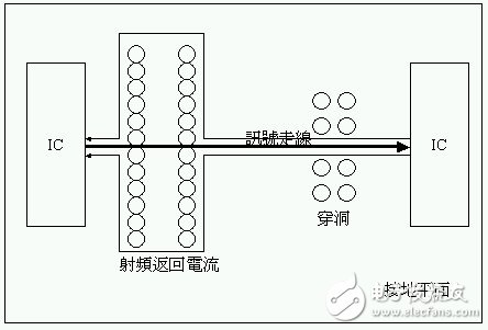
Figure 7: Ground loop when using piercing components
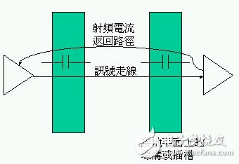
Figure 8: Capacitance makes it possible for RF return currents to pass through the "ditch"
Outdoor low power LED lamps,Aluminum Alloy LED lamps,LED Flood light series
Kindwin Technology (H.K.) Limited , https://www.ktlleds.com