In September 2017, Apple introduced the new model iPhone X of the 10th anniversary edition. The 3D-sensing face recognition it carries has become a new feature of smart phones in the industry. After the launch of the iPhone X, although it has repeatedly been exposed to poor sales, but recently released by Apple in the second quarter of fiscal year 2018 earnings to eliminate market doubts, financial reports showed a total of 52.2 million units sold, higher than the same period last year. And because of the success of the iPhone X, Apple is expected to introduce front-end 3D sensing into the iPad and all new iPhone products in 2018. In this trend, global Android mobile phone manufacturers will certainly accelerate the adoption of 3D sensing technology, making 3D sensing the most likely standard for smart phones in the next five years.
The 3D sensing core components used in the iPhone X include dot matrix projectors, proximity sensors, and floodlights. As shown in Figure 1, the "bangs" part of the iPhone X's front screen, which is where the 3D sensing system and the front camera are mounted, is NIR camera sensor, proximity sensor, floodlight, and spectrum from left to right. Sensors, RGB cameras, and dot matrix projectors.
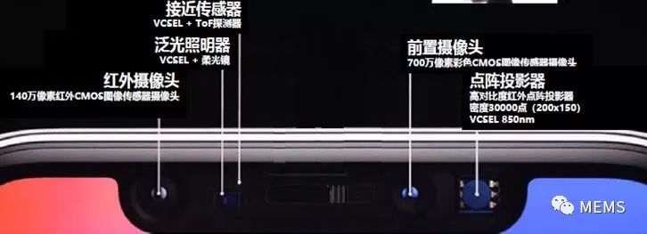
Figure 1 3D sensing component layout for iPhone X
The iPhone X Infrared Dot Matrix Projector is implemented using VCSEL (Vertical Cavity Surface Emitting Laser) diodes with active diffractive optics and folding optics. Figure 2 shows the package structure of this dot matrix projector: VCSEL chip is mounted on an aluminum nitride DPC ceramic substrate, and the aluminum nitride substrate is mounted on the bottom of an HTCC ceramic base. The electrodes of the active diffractive optical element and the IC in the ceramic substrate are connected by metal connectors on the side of the module. When the system is working, an infrared beam is emitted by the VCSEL chip, guided to the active diffractive optical element through the folded optical element, and then the active diffractive optical element separates the beam into a 30,000 spot beam. This very unique assembly scheme achieves optimal thermal management performance and provides higher alignment accuracy for all optical components.
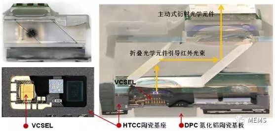
Figure 2 iPhone X infrared dot matrix projector package structure
The Apple iPhone X floodlights and ToF proximity sensors are located above the main speakers and are housed in an optical LGA package, as shown in Figure 3. The floodlighter uses a near-infrared VCSEL chip, which is also mounted on an aluminum nitride DPC ceramic substrate, and emits auxiliary infrared light to ensure that the system operates normally in dark or dark environments. The ToF proximity sensor is responsible for detecting the direct distance between the user and the mobile phone. When the user is too close to the mobile phone, for example, when the user is answering the call, the screen is automatically closed.
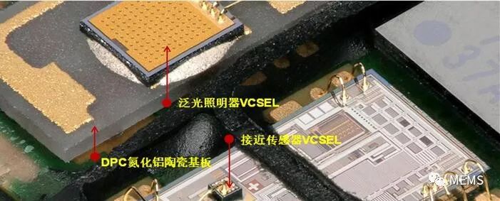
Figure 3 iPhone X floodlights and proximity sensor package structure
By dissecting the iPhone X 3D sensing core element, we found that its two high-power VCSEL chips are all packaged on a high thermal conductivity aluminum nitride DPC ceramic substrate to achieve mechanical support, vertical electrical connection (insulation), efficient heat dissipation, and auxiliary Glowing and other functions.
We believe that using this unique package form is based on the following two points: First, the VCSEL chip for 3D sensing is a vertical structure, the power is above 1W, but the photoelectric conversion efficiency is only about 30%, and most of it becomes hot. Need to emancipate as soon as possible; Second, VCSEL chip power density is very high, need to consider the chip and the thermal stress mismatch caused by the substrate. Therefore, the realization of efficient heat dissipation, thermoelectric separation, and thermal expansion coefficient matching are important considerations in the selection of VCSEL component packaging substrates.
DPC ceramic substrates greatly satisfy this packaging requirement for VCSEL components. DPC ceramic substrate, also known as direct copper plated ceramic substrate, is a technology that combines thin film lines and electroplating process. It adopts image transfer method to make lines on thin-film metalized ceramic plate, and then adopts perforated electroplating technology to form high-density double-sided wiring room. Vertical interconnections. Due to the use of semiconductor micromachining technology, the line width of the substrate can be reduced to 10-30um, the surface flatness is high (<0.3um), the line alignment accuracy is high (±1%), and the high insulation, high thermal conductivity nitrogen Due to the aluminum ceramic substrate, the DPC ceramic substrate possesses many characteristics such as high thermal conductivity, high insulation, high line accuracy, high surface flatness, and coefficient of thermal expansion matching with the chip, and it quickly occupies an important position in the packaging of high-power VCSEL components. Figure 4 shows the VCSEL package structure using a DPC ceramic substrate.
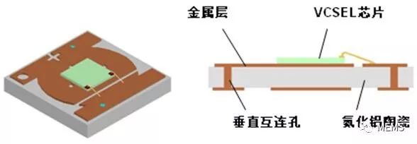
Figure 4 VCSEL package structure using DPC ceramic substrate
Further dissecting the iPhone X infrared dot matrix projector, it was found that the aluminum nitride substrate on which the VCSEL chip was mounted and the HTCC ceramic base were adhered using organic adhesives, as shown in FIG. 5 . This method of bonding with two different ceramic materials, the original intention is to facilitate the optical alignment, but obviously increased the difficulty and reliability of the assembly of the lattice projector (silica gel aging under long-term heating), I think this The limitations of the HTCC ceramic packaging solution are just verified: this solution is a measure of frustration after balancing the high thermal and low-cost requirements. Because HTCC ceramic bases are made of aluminum nitride, the cost is very high, and the process is not mature. If alumina materials are used, the thermal conductivity cannot meet the requirements. Therefore, the aluminum nitride base plate and the HTCC base plate have been pasted. Balanced solution together.
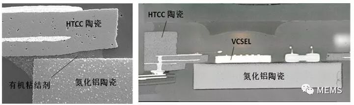
Figure 5 VCSEL package drawing of HTCC ceramic base with DPC ceramic substrate
In addition, high-power VCSEL chips will use eutectic technology to achieve a highly reliable connection with the bottom substrate. The resolution and surface flatness of the HTCC ceramic susceptor using the silk screen process obviously cannot meet the eutectic process requirements. Therefore, the author believes that the current packaging base option for VCSEL components used in the iPhone X-ray infrared dot matrix projector still has a lot of room for improvement.
In view of this potential problem, the 3D molded DPC ceramic substrate developed by Dongguan Kaiyidede Electronic Technology Co., Ltd. (Kayide) will be a better solution. As shown in FIG. 6 , the bottom material of the 3D formed DPC ceramic substrate is a high thermal conductivity aluminum nitride ceramic, and the metal frame is integrally formed on the surface of the ceramic substrate to form a ceramic-metal 3D sealing structure. Compared to the aluminum nitride ceramic and HTCC pedestal mounting solutions used in the iPhone X, the advantages are:
First, the circuit layer at the bottom of the substrate still retains the technical advantages of high resolution, high flatness, and high reliability of vertical interconnects that are unique to DPC ceramic substrates. It is suitable for vertical eutectic welding and eliminates the dimensional accuracy of thick film substrates such as LTCC/HTCC. High, rough lines and other defects;
Secondly, in the process of manufacturing the substrate, the metal frame and the ceramic substrate are integrally formed and tightly combined, which avoids problems such as extra bonding procedures and coordination accuracy in the post-assembly process, and the reliability problems caused by the aging of the glue.
Thirdly, the base material can be arbitrarily selected according to the needs of the package, such as high thermal conductivity aluminum nitride, high-strength silicon nitride, high-purity aluminum oxide and other ceramic materials, and fully realize the thermoelectric separation structure;
Fourth, the manufacturing process is roughly the same as that of the existing DPC ceramic substrate. The product development cycle is short, the consistency is good, and the cost is low.
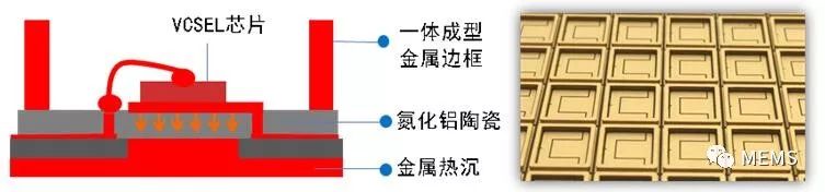
Figure 6 VCSEL packaging diagram using 3D molded DPC ceramic substrate
It can be seen that the package structure has good thermal conductivity, high airtightness, flexible pattern design, and metal frame adopts modular manufacturing, which facilitates large-scale production, especially low cost, short new product development cycle, and high high-power VCSEL devices. Reliable packaging provides a more complete solution.
As the global leader in mobile phones, Apple is the first to adopt 3D sensing technology on its smartphones to completely activate 3D sensing in the consumer market. Apple generously paid 390 million U.S. dollars to increase production of VCSELs in Finisar, DOE optical component supplier AMS 2017, dual counter-attack of stocks, and Osram's acquisition of U.S. VCSEL manufacturer Vixar etc. Market behavior confirmed the high recognition of the global market for 3D sensing VCSELs.
It is reported that, in addition to the front 3D sensing, Apple's follow-up models are expected to increase the post-positioning 3D sensing technology, which means that the market demand for VCSEL 3D sensors will increase exponentially. Since the rear VCSEL 3D sensor requires higher power than the front-end 3D sensor in order to achieve a longer throw distance, it will bring greater heat dissipation and cost challenges. In the long term, VCSEL 3D sensing market has huge potential for growth due to application trends such as Internet of Things and cloud computing, especially in areas such as AR, automotive night vision, autopilot, and industrial vision.
In this context, Kaydeid's DPC ceramic substrate is an excellent solution for high-heating, high-reliability, and low-cost packaging of 3D-sensed VCSEL components. It will surely benefit from the dividends brought by the 3D sensing market explosion and usher in excellent results. Market opportunity period. In addition, Kayde 3D molded DPC ceramic substrates have been extensively patented in mainland China, Taiwan, South Korea, Japan, Europe and the United States and other countries, to enable camera module manufacturers to avoid related patent disputes and achieve high accuracy of 3D sensing elements. , high cost performance, provides a strong guarantee.
ZGAR Disposable Vape
ZGAR electronic cigarette uses high-tech R&D, food grade disposable pod device and high-quality raw material. All package designs are Original IP. Our designer team is from Hong Kong. We have very high requirements for product quality, flavors taste and packaging design. The E-liquid is imported, materials are food grade, and assembly plant is medical-grade dust-free workshops.
Our products include disposable e-cigarettes, rechargeable e-cigarettes, rechargreable disposable vape pen, and various of flavors of cigarette cartridges. From 600puffs to 5000puffs, ZGAR bar Disposable offer high-tech R&D, E-cigarette improves battery capacity, We offer various of flavors and support customization. And printing designs can be customized. We have our own professional team and competitive quotations for any OEM or ODM works.
We supply OEM rechargeable disposable vape pen,OEM disposable electronic cigarette,ODM disposable vape pen,ODM disposable electronic cigarette,OEM/ODM vape pen e-cigarette,OEM/ODM atomizer device.


Disposable E-cigarette, ODM disposable electronic cigarette, vape pen atomizer , Device E-cig, OEM disposable electronic cigarette
ZGAR INTERNATIONAL(HK)CO., LIMITED , https://www.oemvape-pen.com