introduction
DP83848C is a 10/100 Mbps single physical layer (PHY) device with good robustness, full function and low power consumption produced by National Semiconductor Corporation. It supports MII (media independent interface) and RMII (reduced medium independent interface), making the design simpler and more flexible; at the same time, it supports 10BASE ~ T and 100BASE-TX Ethernet peripherals, which is well compatible with other standard Ethernet solutions Sex and versatility.
MII (Medium Independent InteRFace) is a medium-independent interface specified by IEEE802.3u. Its main function is to connect the standard Ethernet interface between the media access control layer (MAC) sublayer and the physical layer (PH-Y), and is responsible for MAC and Communication between PHY. Because MII requires up to 16 signal lines, the resulting I / O port requirements and power consumption are large, and it is necessary to simplify the number of MII pins. Therefore, RMII (Reduced Medium Independent Interface) is proposed. ), The simplified MII.
1 Hardware design
1.1 Circuit design
The receiving and sending lines of DP83848C are each a pair of differential lines, which are connected to the network line after passing through an Ethernet transformer with a transformation ratio of 1: 1. The main functions of the Ethernet transformer are impedance matching, signal shaping, network isolation, and filtering noise from both the network and the device. Typical applications are shown in Figure 1.
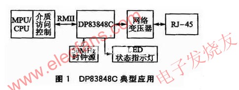
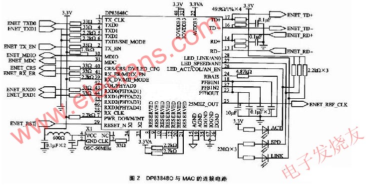
Figure 2 is the connection circuit between DP83848C and MAC. Among them, Xl is an active oscillator of 50 MHz.
1.2 PCB layout
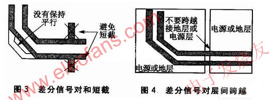
For layout, a 19.9% ​​precision 49.9 Ω resistor and a 100 nF decoupling capacitor should be placed close to the PHY device and through the shortest path to the power supply. As shown in Figure 3, two pairs of differential signals (TD and RD) should be routed in parallel to avoid short stubs, and try to ensure that the length is matched to avoid common mode noise and EMI radiation. Ideally, there should be no crossovers or vias on the signal line, which will cause impedance discontinuity, so its number should be minimized; at the same time, the differential line should be as far as possible, and the signal should not be The line spans the divided plane, as shown in Figure 4. Signals crossing a divided plane will cause unpredictable loop current, which is likely to cause deterioration of signal quality and EMI problems. Note that in Figures 3 and 4, the shaded part is the wrong method.
2 RMll mode description
The RMII mode reduces the connection pins of the PHY while maintaining the existing characteristics of the physical layer device.
RMII is composed of reference clock REF_CLK, transmission enable TX_EN, transmission data TXD [1: 0], reception data RXD [1: 0], carrier sense / reception data valid CRS_DV and reception error RX_ER (optional signal). On this basis, DP83848C also increases the RX_DV receive data valid signal.
2. 1 REF_CLK——Reference clock
REF_CLK is a continuous clock that provides timing reference for CRS_DV, RXD [1: O], TX_EN, TXD [1: O], RX_DV, and RX_ER. REF_CLK is provided by the MAC layer or external clock source. The REF_CLK frequency should be 50 MHz ± 50 × 10-6, with a duty cycle between 35% and 65%. In RMII mode, data is transferred 2 bits at a time with a clock frequency of 50 MHz. Therefore, RMII mode requires a 50 MHz active oscillator (not a crystal oscillator) connected to the X1 pin of the device.
2.2 TX_EN——Transmit enable
TX_EN indicates that the MAC layer is putting the double-bit data to be transmitted on TXD [1: O]. TX_EN should be synchronously confirmed by the first nibble of the preamble, and remain confirmed during the loading of all pending double-bit signals. Before the first rising edge of REF_CLK following the last 2 bits of a frame of data, the MAC needs to invert TX_EN. The change of TX_EN is synchronous with respect to REF_CLK.
2.3 TXD [1: 0] —— Send data
The conversion of TXD [1: O] is synchronous with respect to REF_CLK. After TX_EN is valid, PHY takes TXD [1: 0] as the sending end.
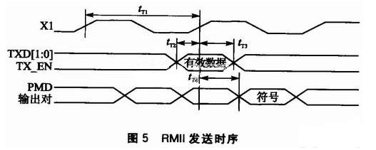
In 10 Mbps mode, the frequency of REF_CLK is 10 times the data rate in 10 Mbps mode. Therefore, the value on TXD [1: 0] must remain stable during 10 pulses to ensure that the DP83848C can sample every 10 cycles. The transmission timing is shown in Figure 5, and the transmission delay is listed in Table 1. Among them, PMD is a physical media depen-dent interface.
2.4 RXD [1: 0] —— Receive data
RXD [1: 0] conversion is synchronized with REF_CLK. In each clock cycle after CRS_DV is valid, RXD [1: O] receives two bits of recovered data from DP83848C. In some cases (such as before data recovery or an error occurs), the predetermined value of RXD [1: O] is received instead of the recovered data. After the confirmation of CRS_DV is released, RXD [1: O] is "00", indicating that it enters the idle state. After CRS_DV is confirmed, before generating the correct receive decoding, DP83848C will ensure that RXD [1: 0] = “00â€.
The recovery data provided by DP83848C is always in the form of nibbles or paired double-bit signals, which is true for all data values ​​starting from the preamble. Because CRS_DV is asynchronously confirmed, it cannot be assumed that the "00" data before the preamble will be in the form of a two-bit signal.
In 100 Mbps mode, confirm in CRS_DV
In the subsequent normal receiving process, RXD [1: O] will remain "00" until the receiver detects the correct start string delimiter (STart St-ream Delimiter, SSD). Once the SSD is detected, the DP83848C will drive the preamble ("01"), followed by the Start of Frame. Delimiter (SFD) ("01" "01" "01" "11"). The MAC should start the data after SFD. If a reception error is detected, RXD [1: 0] will be replaced with the reception string "01" before the carrier activity ends. And because the remaining data in the frame is replaced, the MAC parity will reject the wrong packet. If a wrong carrier (bad SSD) is detected, RXD [1: O] will be replaced with "10" until the end of the reception event. In this case, RXD [1: O] will change from "00" to "10" without indicating the leading character ("01").
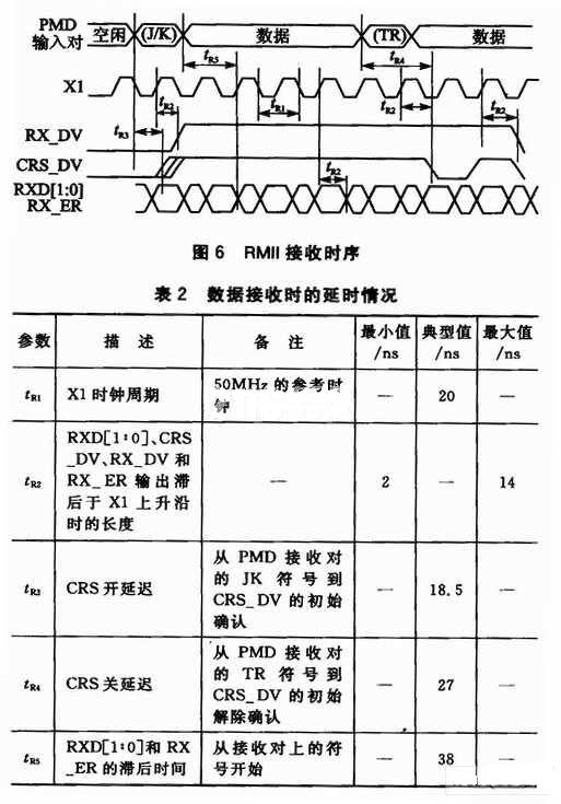
In 10 Mbps mode, after CRS_DV is confirmed, RXD [1: O] will remain "00" until the DP83848C has a recovery pulse and can decode the received data. When there is valid received data, RXD [1: O] receives the recovered data value with "01" as the preamble. Because the REF_CLK frequency is 10 times the data rate in 10 Mbps mode, the MAC samples the value on RXD [1: 0] every 10 cycles. The receiving timing is shown in Figure 6, and the receiving delay is listed in Table 2.
2.5 RX_DV-receive data is valid
Although RMII does not require it, DP83848C still provides a RX_DV signal. RX-DV is a Receive Data Valid signal that does not incorporate CRS. When the first correct recovery data (preamble) or pseudo carrier detection arrives, RX_DV is confirmed, and the confirmation is released after the last two bits of the recovery data are transmitted. By using this signal, the full-duplex MAC no longer needs to recover the RX_DV signal from the CRS_DV signal.
2.6 CRS_DV——Carrier sense / receive data is valid
When the receiving medium is in a non-idle state, the PHY confirms CRS_DV. In carrier detection, CRS_DV is asynchronously confirmed according to the standards related to the working mode. In 10BASE_T mode, this event occurs when the squelch passes. In 100BASE-TX mode, this event occurs when two non-adjacent zero values ​​are detected in 10 bits.
As mentioned in the RMII specification (version 1.2), carrier loss will cause CRS_DV de-acknowledgement synchronized with the REF_CLK cycle, which appears in the first two bits of the RXD [1: O] nibble (ie, CRS_DV is only deactivated on the nibble boundary confirm). After the first confirmation of CRS_DV, if DP83848C still has data bits to be added to RXD [1: O], then during the REF_CLK period, DP83848C should confirm CRS_DV on the second double bit of each half byte, and The first double bit of a nibble is released for confirmation. In this way, from the beginning of the nibble boundary to the end of CRS (Carrier Sense / Received Signal) before RX_DV, CRS_DV rolls over at 25 MHz (100 Mbps mode) or 2.5 MHz (10 Mbps mode) At the end of the DP83848C there are still data bits to be transmitted).
DP83848C can be well compatible with the RMII specification (version 1.0) through programming. In this mode, CRS_DV will asynchronously confirm with CRS, but the confirmation will not be released until the last data is transmitted, and CRS_DV will not be flipped at the end of the packet. Although this mode cannot accurately recover the CRS signal from CRS_DV, it can make the design of the MAC layer simpler.
During the wrong carrier activity time, CRS_DV remains confirmed. Once CRS_DV is confirmed, the data on RXD [1: O] can be considered valid. However, since the confirmation of CRS_DV is asynchronous with respect to REF_CLK, the data on RXD [1: 0] should be "00" before the received signal is decoded correctly.
2.7 RX_ER-receive error
According to the provisions of IEEE802.3 standard, DP83848C provides an RX_ER output. RX_ER can maintain one or more REFCLK cycles to identify an error that has occurred during the current PHY to frame transmission process (MAC sublayer may not be able to detect, but the PHY can detect coding errors or other errors). The change of RX_ER is synchronous with respect to REF_CLK.
Since DP83848C interferes with RXD [1: O] by replacing the original data with fixed data, MAC does not need RX_ER, and only CRC check (that is, parity check) can detect errors.
2.8 Conflict detection
RMII does not provide MAC with a conflict flag. For half-duplex operation, the MAC must generate its own collision detection from the CRS_DV and TX_EN signals. To achieve this, the MAC must recover the CRS signal from the CRS-DV signal and perform a logical AND with TX_EN. Note that CRS_DV cannot be used directly because CRS_DV may be triggered at the end of the frame to mark CRS de-acknowledgement.
3 RMII mode configuration
The DP83848C's RMII mode configuration includes both hardware and software aspects.
3.1 Hardware configuration
As shown in Fig. 2, DP83848C X1 (34) foot provides a 50 MHz CMOS level oscillation signal. At power-on and reset, force DP83848
C enters RMII mode. The method is to connect a pull-up resistor to RX_DV / MII_MODE (pin 39).
3.2 Software configuration
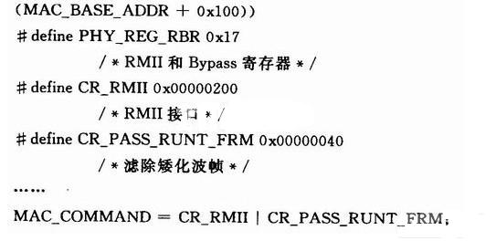
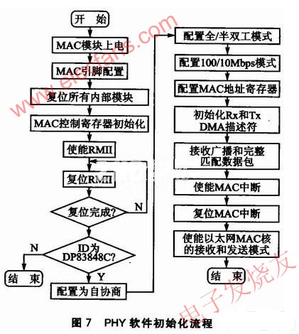
The software initialization flow of PHY is shown in Figure 7.
Conclusion
DP83848C provides a connection scheme with the RMII standard interface, which can reduce the number of pins required from the MAC to the PHY interface. This solution enables design engineers to reduce system design costs while maintaining all the features in the IEEE802.3 specification. Because of this, DP83848C can better adapt to industrial control and factory automation, as well as general embedded systems and other applications.
Impedance Control Pcb,Impedance Board Circuit Board,Impedance Control Board Circuit Board,Impedance Control Board
Shenzheng Weifu Circuit Technology Co.Ld , https://www.viafoem.com