In the field of electronic information, function generators (signal sources) are general-purpose devices. In recent years, the rapid development of electronic information skills has made the requirements for signal sources in various fields constantly improving. Not only the frequency stability and accuracy are required, but also the convenience of frequency modification is required, and it is also required to generate an arbitrary waveform and output signals of different amplitudes. There are many ways to achieve frequency synthesis, but they can basically be summarized into two major categories: direct frequency synthesis and indirect frequency synthesis. It is almost impossible to achieve the above requirements with traditional frequency synthesis skills. DDFS skills are a new type of direct frequency synthesis skill that emerged in the 1970s. The DDFS skill is proposed based on the sampling theorem of the signal. Starting from the concept of “phaseâ€, the frequency synthesis is performed, which not only can use the high frequency stability and high precision of the crystal oscillation, but also has convenient frequency modification and fast conversion speed. It is easy to generate arbitrary waveforms, etc. Therefore, DDFS skills are the core skills of current high-precision signal sources. At present, there are dedicated DDFS chips, such as AD9850 of AD Company of the United States, which can be used for the development of DDS signal sources, but the cost is high.
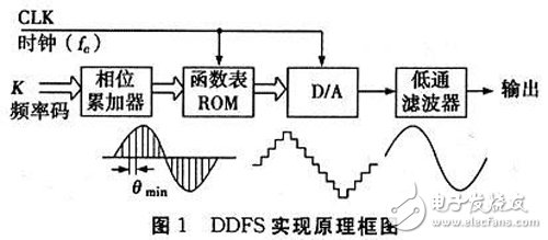
1 DDFS principleThe principle of DDFS: The sampled quantized data of various signals such as sinusoids is stored in the ROM memory. Under the control of the clock, the data in the ROM is read sequentially or at intervals, and then the D/A conversion chip and the subsequent stage are passed. A low-pass filter to achieve a method of frequency synthesis. Its principle block diagram is shown in Figure 1. The main components include: a phase accumulator (also understood as a read address generation unit of a ROM memory cell), a sinusoidal signal sampled quantized data storage ROM table, a D/A conversion, and a low pass filter.
DDFS parameter calculation: The main parameters of DDFS include the sampling points of the sinusoidal signal, the highest output frequency fomax, the lowest output frequency fomax and the frequency resolution Δfo. According to the DDFS principle, when all ROM storage data are sequentially read under clock control, the output signal period is the longest Tomax=NTc, that is, the output frequency is at least fomax; read only two points (âˆ/2 and 3âˆ/ 2) The sampling data, the output signal period is the shortest Tomin=2Tc, that is, the output frequency is up to fomax. Where Tc is the clock period. The corresponding calculation is as follows.
(1) The frequency of the output signal is: fo=Sfc/2n, where 2n is the number of sampling points N, so it can be seen that n is the address digit of the ROM after sampling; where S is the step length, that is, one for each S address Sampling point;
(2) output minimum frequency
(3) Output the highest frequency
View the original image (larger image) Although according to the Nyquist sampling theorem, sampling two points in one cycle can ensure that the spectrum information of the signal is not lost, but for the output signal to be less filtered, the sampling is at least 8 points in one cycle; Therefore, it can be seen that the value range of S should be 1~2n-3;
(4) Frequency resolution Δfo: Δfo=fc/2n, which is consistent with the lowest frequency.
This design makes full use of the on-chip resources of the CycloneII series FPGA chip EP2C35 to implement a DDFS-based sinusoidal signal source. Since the on-chip usable ROM unit of this chip is 483, 840 bits binary, the on-chip ROM resources can only store 215 (32768) 8-bit binary sample points of data.
(1) ROM resource optimization: Since it is a sinusoidal signal, as long as the function value in the (0, n/2) interval is sampled, the corresponding function value in other intervals can be obtained according to its periodicity and symmetry. Therefore, although the on-chip resources can only store 215 (32,768) 8-bit binary data, but using the symmetry of the sinusoidal signal, 217-point sampling can be achieved. Since the sinusoidal signal is negative between (n and 2n), it is necessary to perform a complement conversion when outputting the function value;
(2) Address bit length: The addressed address of the ROM is a 15-bit binary number;
(3) Step bit length: The step size should be 217/23=214, that is, the step is 14-bit binary number;
(4) Phase control word: Phase refers to which interval on (0, 2n) should be recorded when reading data, since there are 4 different intervals. Therefore, a binary number of 2 bits can be used for identification; different phase intervals determine the reading direction of the address and the output function value can not be used for complementary code operations;
(5) Arbitrary waveform generation: To generate an arbitrary waveform, a Fourier series decomposition expression of an arbitrary waveform such as a rectangular pulse, a triangular wave, a sawtooth wave, or the like can be used, and a harmonic is performed by a finite number of times (for example, 10 times). It can be generated by storing it in the specified RAM unit and reading the data in sequence. It is also possible to perform sampling on the data of the corresponding waveform, store it in the ROM, and perform reading in a certain step. Through the above analysis, the full use of the on-chip memory cell, without extending the external memory, the address clock is 10 MHz, the frequency resolution is Δf=78 Hz, the highest frequency of the output signal (minimum sampling of 8 points in one cycle) For fomax=fc/8=1.25 MHz; the lowest frequency of the output signal is fomin=Sfc/2ns=1=fc/217=78 Hz. If the sampling point reaches 232 and above, the frequency resolution can be achieved at 0.015 Hz, reaching the order of mHz. It can be seen that the Cyclone II series chip is used to design a signal source with excellent performance.
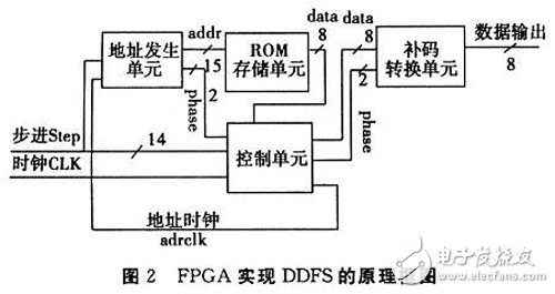
3 DDFS FPGA implementationAccording to the principle of DDFS, its FPGA design principle is shown in Figure 2. The control unit is composed of a finite state machine. Although the control of the whole system does not necessarily need to use the finite state machine, since the FPGA chip used does not support the asynchronous ROM, it is latched from the address into the ROM unit, and the data is read from the ROM for at least one clock cycle or more. . Therefore, the state machine is used to perform the control, and a better output and clock synchronization can be achieved. The control flow is: the clock signal enters the control unit, and the input clock adrclk of the address generation unit is generated by the address generation unit, and the address generation unit is combined with the input step signal Step to generate the address and the quadrant corresponding to the address, driven by the clock adrclk, After the address is generated, it is input to the ROM unit immediately. After two clock cycles, the control unit reads the data corresponding to the input address from the ROM storage unit, and under the control of the clock, the previously generated quadrant Phase and The ROM data is sent to the complement conversion unit together, and the complement conversion unit determines that the complement conversion cannot be performed according to the value of Phase. If necessary, the complement operation is performed and the data is output. If not, the data is directly output. . Detailed design details of each module are given below.
High Quality Rectifier Diode with Competitive Price, Fast Shipping, Order Now.Years of experience.
The company has domestic advanced diode production equipment, complete testing methods and quality assurance system.
Advanced Technology.Electronic component diodes are widely used in household appliances, green lighting, network communications, power chargers, automotive electronics and other fields.

Rectifier Diode,diode Bridge Rectifier,KBU Bridge Rectifiers,rectifier diode,Fast rectifier diode
Changzhou Changyuan Electronic Co., Ltd. , https://www.cydiode.com