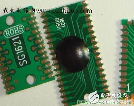
When doing small electronic production, you will see small black round "pimples" on some circuit boards, as shown in the figure below, especially on various voice chips.
So what exactly are these small round "pimples"?
This is called "bonding" or COB (chiponboard).
Simply put, it is to make the used chip directly on the circuit board, and then drip some black epoxy glue to seal the "core" of the chip. The sealed chip can be a common chip or a chip customized by the manufacturer.
It may be one chip or multiple chips. The internal structure is invisible without removing the epoxy glue.
But once the epoxy resin is cured, it is difficult for you to remove it. If it becomes hard, it will damage the chip inside. Moreover, even if you remove all the epoxy resin to clean, you can only see a piece of "silicon board" (that is, the chip's "Core"), lead some wires to the circuit board. The model number is almost impossible to find, unless you are familiar with the circuit you disassembled.
For in-depth understanding, see below:
The COB process refers to a process in which bare chips are directly pasted on a printed circuit board, followed by wire bonding, and then the chip and leads are encapsulated and protected with organic glue. Compared with the conventional process, the packaging density of this process is high and the process is simple and convenient.
COB process flow and basic requirements
Process flow and basic requirements
Clean PCB---Drip Adhesive Adhesive---Chip Paste---Test---Heat Sealing Adhesive Curing---Test---Warehouse
1. Clean the PCBThe cleaned PCB board still has oily dirt or oxide layer and other dirty parts. Use a skin wipe to test the positioning or test the needle position to wipe the PCB board with a brush or blow it with an air gun before it can flow into the next process. For products with strict anti-static properties, use an ion blower. The purpose of cleaning is to remove dust and oil stains on the PCB board bonding pads to improve the quality of the bonding.
2. Adhesive glueThe purpose of the adhesive glue is to prevent the DIE from falling off during the transfer and bonding process of the product
Needle transfer and pressure injection are usually used in the COB process
Needle transfer method: Use a needle to take a small drop of adhesive from the container and apply it on the PCB. This is a very fast dispensing method
Pressure injection method: Put the glue into the syringe, apply a certain air pressure to squeeze the glue out. The size of the glue point is determined by the nozzle diameter of the syringe and the pressure time and pressure and is related to the viscosity. This process is generally used in dripping machines or DIEBOND automatic equipment
The size and height of the glue drop depends on the type, size, distance from the PAD position, and weight of the chip (DIE). The size and weight of the chip is larger, and the amount of glue drop should not be too large to ensure sufficient viscosity. At the same time, the adhesive glue can not pollute the bonding pad. If you have to say what standards are there, it can only be determined by different products. If you insist that the height of the chip cannot exceed 1/3 of the chip and the amount of glue cannot be exposed as the standard, there is no need for this.
3. Chip pasteChip pasting is also called DIEBOND (solid crystal) bonding DIE Bang DIE Bang IC and other companies have different names. In chip sticking, the hardness of the vacuum suction pen (suction nozzle) is required to be small (some companies also use cotton swabs for sticking). The diameter of the suction nozzle depends on the size of the chip, and the tip of the nozzle must be flat to avoid scratching the surface of the DIE. When pasting, check the DIE and PCB model and whether the pasting direction is correct. The DIE towel to the PCB must be "smooth and upright". "Flat" means that the DIE and the PCB are parallel and close to each other. In the process, it is not easy to fall off. "Positive" means that the DIE and the reserved position of the PCB are affixed to the front and cannot be twisted. It must be noted that the direction of the chip (DIE) must not be reversed.
4. Bond wire (wire bonding)Bonding (wire bonding) WireBond bonding connection is called differently, here is bonding as an example
Bonding connects the two solder joints of each state line according to the position determined by the BONDING diagram to achieve electrical and mechanical connection. Bonding PCB requires its tensile strength to meet the company's standard (reference 1.0 line greater than or equal to 3.5G, 1.25 line greater than or equal to 4.5G) when bonding the PCB for bonding tensile test, the shape of the aluminum wire solder joint is oval, and the gold wire solder joint shape It is spherical.
Bonding melting point standard
Aluminum wire:
The wire tail is greater than or equal to 0.3 times the wire diameter and less than or equal to 1.5 times the wire diameter
The length of the solder joint is greater than or equal to 1.5 times the wire diameter and less than or equal to 5.0 times the wire diameter
The width of the solder joint is greater than or equal to 1.2 times the wire diameter and less than or equal to 3.0 times the wire diameter
The height of the arc is equal to the height of the parabola of the circle (not too high or too low, depending on the product)
Gold Line:
Solder balls are generally about 2.6-2.7 times the wire diameter
During the bonding process, handle with care, and the points must be accurate. The operator should observe the bonding process with a microscope to see if there is any disconnection, winding, offset, hot and cold welding, aluminum lifting, etc., and other defects, if any Then immediately notify the management or technical staff. Before the formal production, there must be a first inspection by a special person to check whether there are any faults, few states, and missing states. Every 2 hours, there should be someone to check its correctness.
5. Plastic closuresSealing glue mainly applies black glue to PCB boards that are tested OK. When dispensing glue, pay attention to that the vinyl should completely cover the PCB sun circle and the aluminum wire of the bonding chip. There should be no exposure. The vinyl should not be sealed out of the sun circle and other places. There is vinyl, if there is leakage of glue. Wipe off the cloth strips instantly. During the entire dispensing process, the needle or the wool stick should not touch the DIE and the bonded wire. The surface of the dried vinyl shall not have pores or uncured vinyl. The height of the black glue should not exceed 1.8mm, and the special requirement should be less than 1.5mm. The temperature of the preheating plate and the drying temperature should be strictly controlled during dispensing. (Zhenqi BE-08 vinyl FR4PCB board as an example: the preheating temperature is 120±15 degrees, the time is 1.5-3.0 minutes, the drying temperature is 140±15 degrees, and the time is 40-60 minutes) The sealing method usually also adopts needle transfer Method and pressure injection method. Some companies also use glue dispensers, but their cost is relatively high and their efficiency is low. Usually, cotton swabs and syringes are used for glue, but the operators must have skilled operation ability and strict process requirements. If the chip is damaged, it will be very difficult to repair it. Therefore, this process management personnel and engineering personnel must be strictly controlled.
6. testDue to some undesirable phenomena such as wire breakage, wire winding, false soldering, etc. during the bonding process, which may cause chip failure, the chip scale package must be tested for performance
According to the detection method, it can be divided into two categories: non-contact detection (inspection) and contact detection (test). Non-contact detection has developed from manual visual inspection to automatic optical image analysis (AOI) X-ray analysis, from appearance circuit pattern inspection Developed to the quality inspection of the inner layer solder joints, and developed from a single inspection to a combination of quality monitoring and defect repair.
Although the bonding machine is equipped with an automatic wire bonding quality inspection function (BQM), the automatic bonding wire quality inspection of the bonding machine mainly adopts two methods of design rule detection (DRC) and pattern recognition. DRC is to check the quality of the welding wire according to some given rules, such as how much the melting point is less than the wire diameter or how much greater than some set standards. The pattern recognition method compares the stored digitized image with the actual work. But this is all affected by process control, process regulations, parameter changes, etc. The specific method used should be determined according to the specific conditions of each unit's production line and the product. But no matter what the conditions are, visual inspection is the basic inspection method and one of the contents that COB craftsmen and inspectors must master. The two should complement each other and cannot replace each other.
Perkins Diesel Generator assembly by Perkins diesel engine, alternator, radiator, controller, base frame;
. World Famous diesel engine brand: Perkins
. World famous AC alternator brand: Stamford, Leroy Somer, Mecc Alte, Marathon, Faraday, SWT
. World famous genset controller brand: Deepsea, ComAp, Deif, SmartGen,
. Good Quality Cooling Radiator
. Start Battery system
Perkins Genset,Perkins Generator,Perkins Power Generator,Perkins Diesel Generator
Guangdong Superwatt Power Equipment Co., Ltd , https://www.swtgenset.com