DDR=Double Data Rate double rate synchronous dynamic random access memory. Strictly speaking, DDR should be called DDR SDRAM. People are used to calling it DDR. Among them, SDRAM is an abbreviation for Synchronous Dynamic Random Access Memory, which is Synchronous Dynamic Random Access Memory. This article first introduced the DDR operating principle and structure diagram, followed by the DDR DQS signal processing, specifically follow the small series together to find out.
DDR working principle and structure diagramThe basic principle of DDR
There are many articles that discuss the principles of DDR, but it seems to have no way of getting to the point and even bring up some wrong ideas. Let's first look at a regular DDR timing diagram.
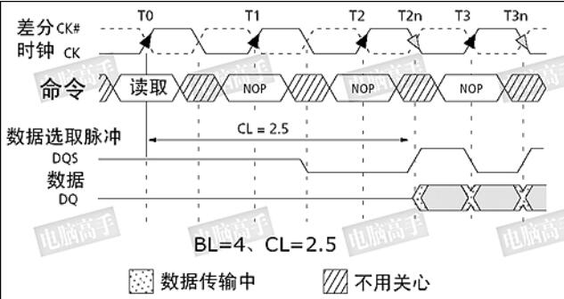
From this it can be found that it has two more signals: CLK# and DQS, CLK# and the normal CLK clock are in the opposite phase to form a differential clock signal. The data transmission is performed at the intersection of CLK and CLK#. It can be seen that both the rising and falling edges of CLK (which happens to be the rising edge of CLK#) all have data to be triggered to realize DDR. Here, we can say that the purpose of DDR is reached through the differential signal, and even CLK# helps the triggering of the second data, but this is only a brief description of the surface phenomenon, which cannot be said from the strict definition. The reason why we can achieve DDR, but also from its internal improvements.
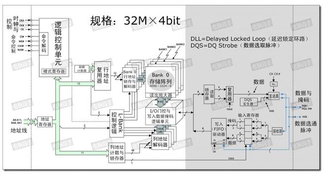
Internal structure of DDR memory chip
This is a 128Mbit memory chip. It can be seen from the figure that the structure of the white area and the SDRAM is basically the same, but please pay attention to the gray area, which is different from the SDRAM. The first is the internal L-Bank specification. The capacity of the L-Bank memory cell in the SDRAM is the same as the bit width of the chip, but not in the DDR SDRAM. The capacity of the memory cell is double the bit width of the chip, so it is no longer possible to apply SDRAM to explain the bit width. Formula for storage unit capacity. Therefore, the actual number of row and column addresses is also different from that of the same specification SDRAM.
Taking this chip as an example, when reading, the L-Bank transfers 8 bits of data to the read latch at the trigger of the internal clock signal, and then divides into 4 channels of data to transfer to the multiplexer. The latter uses them. Combine them into one 4-bit data stream. Then, the transmitter transmits two 4-bit data to the North Bridge on the rising and falling edges of the external clock under the control of the DQS. In this way, if the clock frequency is 100MHz, then at the I/O port, since it is triggered by the upper and lower edges, the transmission frequency is 200MHz.
Now that we basically understand the working principle of DDR SDRAM, this internal memory cell capacity (can also be called the chip internal bus bit width) = 2 × chip width (also known as the chip I / O bus bit width) design The so-called 2-bit Prefetch, and some companies are aptly called 2-n Prefetch (n represents the chip width).
DDR DQS signal processingI. DDR 1 & 2 & 3 bus overview
The full name of DDR is Double Data Rate SDRAM, abbreviated as DDR. Now DDR technology has been developed to DDR3, theoretically speed can support up to 1600MT/s. The number of DDR bus lines is high, the speed is fast, the operation is complicated, and the detection is difficult, which brings a great challenge to the test and analysis.
DDR essentially does not need to increase the clock frequency to double the speed of the SDRAM. It allows data to be read on the rising and falling edges of the clock, and is therefore twice as fast as standard SDRAM. As for the address and control signals, it is the same as the conventional SDRAM, and the data is still judged on the rising edge of the clock.
At present, many computers use DDR2 memory with a clock frequency of 533 MHz. More advanced DDR2 memory is becoming increasingly popular. Its clock frequency is between 400 MHz and 800 MHz, and the new DDR3 memory clock frequency can work between 800 MHz and 16OO MHz. between. DDR3 memory chip has another strength: lower power consumption, its operating voltage is 1.5 volts, lower than 1.8 volts of DDR2 memory chips and 2.5 volts of DDR1 memory chips. Battery life can be extended in devices that use batteries, because the energy consumption is low, the amount of heat generated is also low, so the cooling requirements are lower.
The meaning of several new features of DDR 2 & 3 is: ODT (On Die Termination), DDR1 matching is placed on the motherboard, and DDR2 & 3 is directly designed into the DRAM chip to improve signal quality. The OCD (Off Chip Driver) is a control function for enhancing pull-up and pull-down driving by reducing DQS and /DQS (DQS is a data Strobe, a source synchronous clock, data 1 and 0 are judged by DQS as a clock) Skew (time lag) Increase the Timing Margin of the signal. Posted CAS is a way to increase bus utilization. The AL (Additive Latency) technology is relative to the external CAS. The internal CAS performs a certain delay.
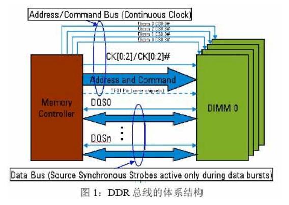
Figure 1 shows the architecture of the DDR bus. Among them DQS is the source synchronous clock, uses DQS to read the corresponding data DQ on the receiving end, the rising edge and the falling edge are all valid. On the DDR1 bus, DQS is a single-ended signal, while DDR2&3, DQS is a differential signal. Both DQS and DQ are tri-state signals that are transmitted in both directions on the PCB trace. During read operations, the edges of the DQS signal are aligned in time with the DQ signal edges. In write operations, the edges of the DQS signal are in timed relation to the DQ. Aligning the center of the signal, refer to Figure 2, this presents a huge challenge for test validation: It is very difficult to separate the "read" signal from the "write" signal!
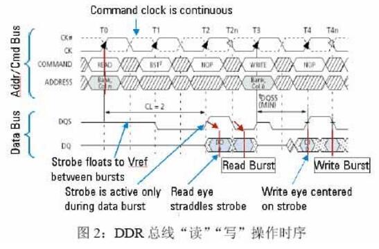
In Figure 2, Addr/Cmd Bus means address/command bus. Both are valid on the rising edge of the clock. The command is determined by: /CS (chip select), /RAS, /CAS, and /WE (write enable). For example, : "Read" command is: LHLH, "Write" command is: LHLL and so on. There are many operation commands, mainly NOP, Active, Write, Read, Precharge, Auto Refresh, or Self Refresh. (For details, please refer to Jedec standard JESD79.) . The Data Bus is a data bus, which judges the 0 and 1 of the data DQ by the rising and falling edges of DQS.
Second, DDR 1 & 2 & 3 bus signal integrity test
The DDR bus PCB has many traces, high speed, complicated operation timing, and it is prone to failure problems. For this reason, we often use an oscilloscope to perform signal integrity test and analysis of the DDR bus. The usual test contents include:
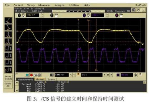
1, command signal waveform and timing parameters: need to test / RAS, / CAS, / WE, / CS signal quality, such as Vmax (maximum voltage), Vmin (minimum voltage), Slew Rate (slope), Ringback ( (Background), etc.; also need to test the Setup Time and Hold Time relative to the clock edge. When testing the setup and hold times relative to the clock edge, it is important to note the location of the reference level and capture of the worst-case waveform. The worst-case setup and hold time values ​​have not been tested in the /CS setup and hold times tests of Figure 3. For this reason, we need to use eye pattern accumulation to find the worst-case setup and hold times. .
2. Waveforms and timing parameters of the address signal: tests of the test content and the test quality and the setup and hold times relative to the clock edges.
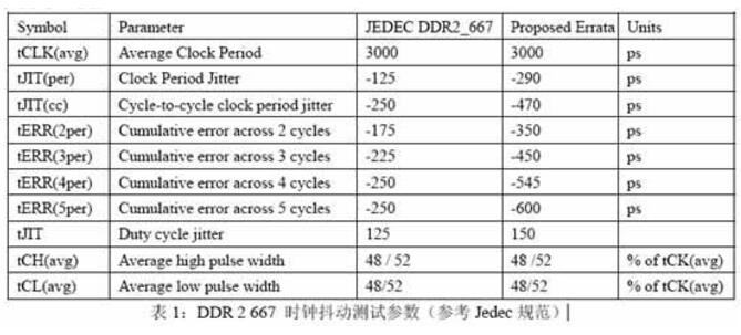
3. Waveform and jitter parameters of the clock signal: The test is recommended to use a differential probe. Waveform parameters include overshoot, undershoot, Slew Rate or Rise Time and Fall Time, high and low time, and Duty Cycle. The clock jitter generally only tests Cycle-Cycle jitter. However, when the rate exceeds 533Mbit/s DDR2&3, the test content is quite large and cannot be ignored. Table 1 below shows the specifications of DDR2 667. The testing of these jitter parameters requires special software.
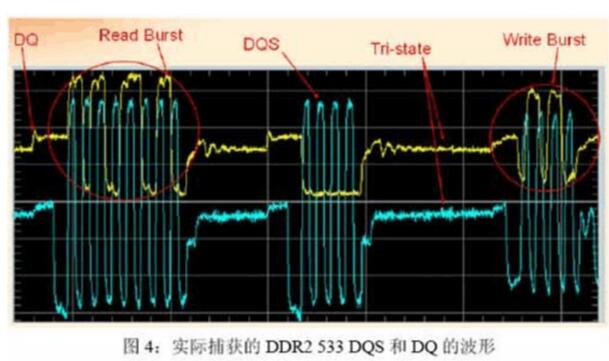
4, speed signal signal waveform and timing parameters: DQS (source synchronous clock) and DQ (data) waveform parameters and command address testing similar to the test is relatively simple, but the detection is more complicated and difficult. DDR1 and DQS are single-ended signals. They can be tested with single-ended probes. DDR2 & 3 DQS are differential signals. It is recommended to use differential probes to reduce the detection difficulty. The timing relationship between DQS and DQ, ie, the relative setup and hold times under different operating conditions is very complex and difficult to analyze. Figure 4 shows the actual captured DDR2 533 DQS and DQ waveforms. The Tri-state characteristics of DQS and DQ, the relative timing characteristics of DQS and DQ for Read Burst and Write Burst can be seen from the figure. In our tests, we only captured such waveforms, and then tested that the setup and hold time parameters in the “read†and “write†operations are not enough because the data pattern is changed and the burst length is also changed. Several timing parameters are difficult to cover in various situations, and it is harder to measure the worst case. Many engineers took a week to test DDR. The key point that still can't detect the problem is here. Therefore, we should use the eye diagram to test the DDR read and write timing, to ensure that the overall timing and capture the worst case waveforms, it is best to apply serial data analysis methods, call the template to help determine.
Third, DR 1 & 2 & 3 "read" "write" eye test
Based on the different characteristics of DDR “read†and “write†signals, I designed a software to perform “read†and “write†eye diagram test analysis. The software uses VEE Pro 7.5 design interface and uses VEE Pro embedded Matlab script to analyze data. The specification-based AC parameter design template helps engineers perform the most complex part of the DDR signal integrity test analysis, namely the “read†and “write†data eye test analysis.
Figure 5 is an example of a software interface and analysis results. The above two graphics are user interfaces. On the left is the offline analysis software, which uses the oscilloscope to simultaneously acquire DQS and DQ signals and save them as *.CSV files. During acquisition, the sampling rate is set to 20 GSa/s, and the storage depth is set to 200 k or more to ensure that enough data is captured. At the same time, the system under test runs a large software or MemoryTest.exe tool (this memory test software can perform the pressurization test of the memory bus. , generally do system design or memory design have), in order to allow enough data on the bus, to increase the possibility of capturing various patterns and the worst case. Off-line software calls the acquired waveform, automatically removes tri-state data, puts “read†data together, puts “write†data together, based on DQS active edge (removes pre-adjusted and post-adjusted rising and falling edges ), accumulate together to form an eye diagram, call the template to determine whether the signal is good or bad and meet the specification requirements.
The upper right panel of Figure 5 is an online real-time analysis software interface based on Agilent's DSO80000 and 54850 series oscilloscopes. The software needs to be installed inside the oscilloscope or installed on an external computer and connected to the oscilloscope using a LAN or GPIB to USB adapter (82357A). The oscilloscope's channel 1 detects DQS, channel 3 detects DQ, and the system under test runs large software or the MemoryTest.exe tool. Enter the number of times you want to repeatedly capture the waveform on the online software, then press “starting†to capture the real-time data and analyze the real-time eye diagram. The software will control the oscilloscope to capture the waveform, then analyze the data to form an eye diagram, and call the template to judge whether the signal is satisfied. The specification requires that the next capture and analysis be repeated while accumulating the newly captured waveform onto the previously captured waveform. The software implemented by the online software is similar to the off-line software, except that it can automatically control the oscilloscope, perform multiple captures and analysis of the waveform, and at the same time display the analysis results of the waveform captured in real time along with the previous results.
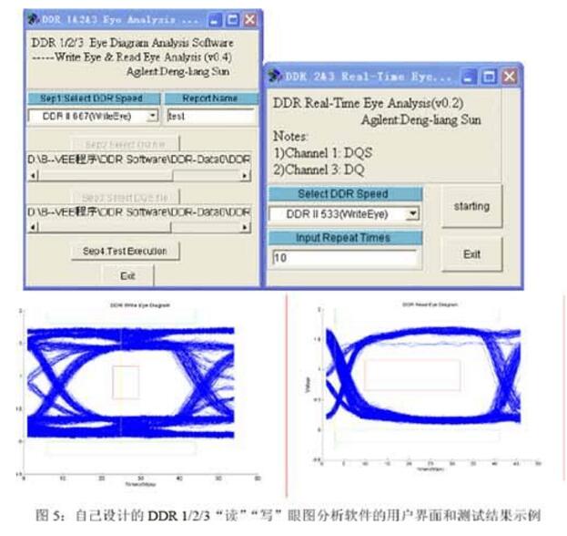
The following two waveforms in Figure 5 are examples of actual analysis results. The analysis is for DDR2 667 and the test points are on the DIMM memory module. What makes sense to us is the “write†eye on the left. It reflects the signal that the signal is sent from the North Bridge and travels to the DRAM receiver chip over a longer distance on the motherboard. This is what we need to do when designing and testing the system. Illustration. The figure on the right shows the waveform of the signal sent directly from the DRAM chip. Because the test point is on the DIMM, it has only reference value for us. When the timing problem is tested at the North Bridge, it is determined by the observation of this waveform that it is a problem of the motherboard design. It is also a problem with DIMMs or DRAM chips themselves. If the test point is at Northbridge, we need to pay attention to "read" eye diagrams, and at this time, "write" eye diagrams are generally only of reference value.
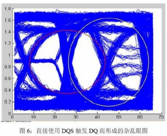
What is the algorithm for this DDR Read & Write eye analysis software? In fact, it is very simple, as shown in Figure 6, if you directly use DQS to trigger DQ, it will form a chaotic eye diagram, but in the middle also includes the required information, as shown in the red circle around the "write" eye diagram information, Around the yellow circle on the way is "read" eye diagram information. The reason why eye diagrams are chaotic is that they include both "tri-state" signals and "read" and "write" signals, and the timing of "reading" and "writing" signals is contradictory. The separation process using software is relatively easy: first, throw away the tri-state signal and retain useful information. In the software design, detect the effective edge of DQS. The signal farther from the effective edge of DQS is the tri-state signal, throw it away; then, according to The relationship between setup time and hold time divides the "read" signal and the "write" signal into two databases; finally, the "read" signal database is put together by the DQS active edges to form an eye diagram and the "write" signal database is valid by DQS. Edges are put together to form eye diagrams, and templates are called to generate test results.
Fourth, DDR 1 & 2 & 3 template definition
The DDR specification does not define a template, which poses a challenge for judging whether the signal meets the specification requirements when analyzing signals in an eye diagram manner. In order to more easily determine whether the requirements of the specification are satisfied, the “read†and “write†eye diagrams are analyzed in the same way as general serial signals. I designed the “read†and “write†templates according to the Jedec specification. The following uses the definition of "write" eye template as an example to introduce the template design method.
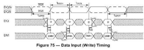
Figure 7 shows the timing and waveform parameters of the Jedec specification. tDS is the settling time relative to the effective edge of DQS, tDH is the hold time relative to the effective edge of DQS, tDS is relative to the AC parameter of DQ, and tDH is relative to the DC parameter of DQ. However, in order to test the convenience, we can use AC parameters to define tDS and tDH. The test of tDS and tDH parameters is the core test parameter of DDR.
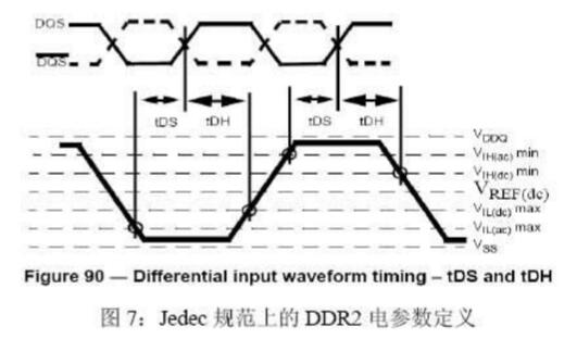
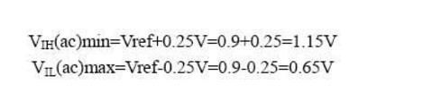
In the Jedec specification, we can find the canonical values ​​of tDS and tDH at various rates, such as DDR2 533, tDS is 100ps, and tDH is 225ps. We can also find AC parameter values ​​at various rates, such as DDR2 533: where VIH(ac)min is the minimum value of the VIH(ac) specification, VIL(ac)max is the maximum value of the VIL(ac) specification, and Vref. The reference voltage is 1.25V for DDR1, 0.9V for DDR2, and 0.75V for DDR3.
Based on the tDS and tDH and VIH(ac)min and VIL(ac)max parameters, we can draw a template for the DDR2 533 “write†eye diagram as shown in Figure 8. The middle red area is the template, Setup time is the tDS setup time, the Hold time is the tDH hold time, VIH(AC) is the VIH(ac)min value, and VIL(AC) is the VIL(ac)max value. The middle yellow line is the effective edge of the DQS, the valid rising or falling edge.
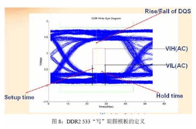
In strict accordance with the specification, the middle template should be defined as a horizontal trapezoid, because the holding time is relative to the DC parameters, but using a rectangle can define a more stringent parameter requirement.
Five, summary
DDR is the most complex bus in the bus that needs signal integrity testing. It not only has many traces, it is difficult to detect, but also the timing is complex. Various operations are intertwined. Based on years of practical experience, this paper provides some reference methods for testing, in particular, puts forward an innovative viewpoint for the definition of test methods and templates for “read†and “write†eye diagrams, and designs the software to implement this method. Motherboard, DIMM, DRAM designers and testers have reference value.
Qiuck deatail:
- Synchronization mechanism for multi-screen playing
- Powerful processing capability
- Comprehensive control plans
- Synchronous and asynchronous dual-mode
- Dual-Wi-Fi mode
Other Hardware Features
- 4 Ethernet ports, loading capacity of each port up to 2,300,000 pixels, with the maximum width of 4096 pixels and maximum height of 1920 pixels
- Wired Gigabit Ethernet
- Stereo audio output
- HDMI Loop
- HDMI input and auto full-screen display
- 2 USB ports allowing for USB playback
- Onboard light sensor connector allowing for automatic and scheduled brightness adjustment
Application:
Movie theaters, clubs, stages.
* Business Organizations:
Supermarket, large-scale shopping malls, star-rated hotels, travel agencies
* Financial Organizations:
Banks, insurance companies, post offices, hospital, schools
* Public Places:
Subway, airports, stations, parks, exhibition halls, stadiums, museums, commercial buildings, meeting rooms
* Entertainments:
Video processor;controller;video controller
Guangzhou Chengwen Photoelectric Technology co.,ltd , https://www.cwstagelight.com