In our application development, there are often some program running parameters that need to be saved, such as some correction factors. The characteristics of these data are: they are small in number and do not need to be modified frequently, but they cannot be defined as constants, because each device may be different and there may be modifications in the future. It is a convenient method to directly store such data in a specified location and modify the value of the storage location directly when it needs to be modified. Considering that the amount of data is relatively small, it is neither economical nor necessary to use a dedicated storage unit, and the internal Flash memory of the STM32F103 is large, and the basic Flash operation function is also provided in the ST library function, which is also convenient to implement. .
Take the large-capacity product STM32F103ZET as an example, its Flash capacity reaches 512K, and some of it can be used as data storage. The following is a large-capacity Flash organization mode:
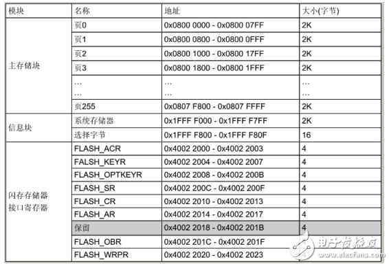
The flash module of STM32 consists of three parts: main memory, information block and flash memory interface register.
1) Main memory, which is used to store code and data constants (such as const type data). For high-volume products, it is divided into 256 pages of 2K bytes per page. Note that small and medium capacity products are only 1K bytes per page. It can be seen from the above figure that the starting address of the main memory is 0X08000000. When both B0 and B1 are connected to GND, the code is run from 0X08000000.
2) Information block, this part is divided into 2 small parts, in which the startup program code is used to store the startup program that comes with ST, which is used for serial port download code. When B0 is connected to V3.3 and B1 is connected to GND, it runs. This is the part of the code. The user selects the byte, which is generally used to configure write protection, read protection and other functions. This chapter does not introduce it.
3) Flash memory interface register, which is used to control flash memory read and write, etc., is the control mechanism of the entire flash memory module. The writing of main memory and information blocks is managed by the embedded Flash Program/Erase Controller (FPEC); the high voltage for programming and erasing is internally generated.
When a flash write operation is performed, any read operation to the flash memory will lock the bus, and the read operation will be performed correctly after the write operation is completed; the code or data read operation cannot be performed while the write or erase operation is being performed.
According to the above Flash organization mode, we can make corresponding definitions according to their own convenience. Since the large capacity is defined as 2K per sector and the small and medium capacities are defined as 1K, we make the following macro definition:
#define FLASH_SIZE 512 //The size of the FLASH capacity of the selected MCU (in K)
#if FLASH_SIZE"256
#define SECTOR_SIZE 1024 //byte#else
#define SECTOR_SIZE 2048 //byte #endif
Although the library functions of ST are more comprehensive, they are all basic operations. In order to use them, they are repackaged according to our own needs.
For read operations, it is relatively simple, the built-in flash module can be directly addressed in the general address space, just like reading variables.
/ / Read multiple data starting from the specified address void FLASH_ReadMoreData (uint32_t startAddress, uint16_t * readData, uint16_t countToRead)
{
Uint16_t dataIndex;
For(dataIndex=0;dataIndex"countToRead;dataIndex++)
{
readData[dataIndex]=FLASH_ReadHalfWord(startAddress+dataIndex*2);
}
}
/ / Read the halfword of the specified address (16-bit data) uint16_t FLASH_ReadHalfWord (uint32_t address)
{
Return *(__IO uint16_t*)address;
}
/ / Read the full word of the specified address (32-bit data) uint32_t FLASH_ReadWord (uint32_t address)
{
Uint32_t temp1, temp2;
Temp1=*(__IO uint16_t*)address;
Temp2=*(__IO uint16_t*)(address+2);
Return (temp2""16)+temp1;
}
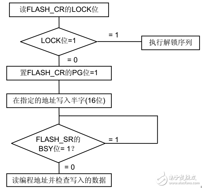
Write operations are much more complicated, and write operations include writing and erasing user data. In order to prevent misoperation, there is also a write protection lock. But these basic operations ST library functions have been written for us, we only need to call.
After STM32 reset, the FPEC module is protected and we can only operate the relevant registers after the write protection is removed. The programming of the STM32 flash must be written to 16 bits at a time, and any operation that is not a halfword will cause an error. The following picture is the process of writing Flash:
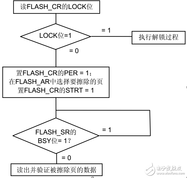
When the FLASH of STM32 is programmed, the FLASH of the write address must also be erased (that is, its value must be 0XFFFF), otherwise it cannot be written. Flash erasure requirements must be erased on a full page, so you must also write the entire page, otherwise you may lose data. The following picture shows the Flash page erase process:
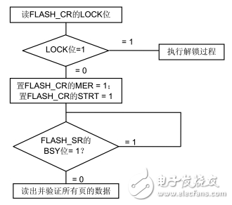
The following is the Flash full erase process,
According to the above illustration, we write the data write function as follows:
/ / Write multiple data from the specified address void FLASH_WriteMoreData (uint32_t startAddress, uint16_t * writeData, uint16_t countToWrite)
{
If(startAddress "FLASH_BASE||((startAddress+countToWrite*2)"=(FLASH_BASE+1024*FLASH_SIZE)))
{
Return;//illegal address}
FLASH_Unlock(); //Unlock write protection
Uint32_t offsetAddress=startAddress-FLASH_BASE; //calculate the actual offset address after removing 0X08000000
Uint32_t sectorPosiTIon=offsetAddress/SECTOR_SIZE; //calculate the sector address, 0~255 for STM32F103VET6
Uint32_t sectorStartAddress=sectorPosiTIon*SECTOR_SIZE+FLASH_BASE; //first address of the corresponding sector
FLASH_ErasePage (sectorStartAddress); / / erase this sector
Uint16_t dataIndex;
For(dataIndex=0;dataIndex<countToWrite;dataIndex++)
{
FLASH_ProgramHalfWord(startAddress+dataIndex*2, writeData[dataIndex]);
}
FLASH_Lock (); / / lock write protection
}
Before erasing, the data on the page should be read out and merged with the data to be written, and then written after being erased, but the amount of data is large (the large capacity is 2K and one sector), so it is considered to be a small amount. Data storage, so all data is written at the same time each time, simplifying operations and reducing data processing. After testing the above program to write and read data are correct, you can achieve internal Flash read and write operations.
Dc Power Contactor,Contactor Relay,Dc Contactor Relay,Dc Magnetic Contactor
NanJing QUANNING electric Co.,Ltd , https://www.quanningtrading.com