The so-called clamp is the output voltage that clamps the input voltage to a peak at a predetermined level without changing the signal.
Clamp circuit (1) function: Move the input signal level up or down without changing the waveform of the input signal. (2) Basic components: diode D, capacitor C and resistor R (DC battery VR). (3) Category: Negative clamp and positive clamp. (4) Note D is assumed to be ideal, and the time constant of RC is also large enough to not distort the output waveform. Any communication signal can produce a clamp. Negative clamp
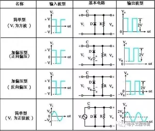
(1) Simple type
Working principle Vi is half a week, DON, C is charged to V value, Vo = 0V. When Vi is negative for half a week, DOFF, Vo=-2V. (2) biased type
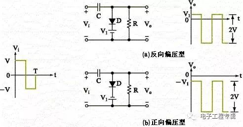
Working principle Vi is half cycle, diodes DON, C are charged to V value (left positive, right negative), Vo = +V1 (a) map or -V1 (b) map. When Vi is negative for half a week, the diode DOFF, the RC time constant is sufficiently large, Vo = VC + Vi (negative half cycle) = 2V. Comparison of several diode negative clamp circuits
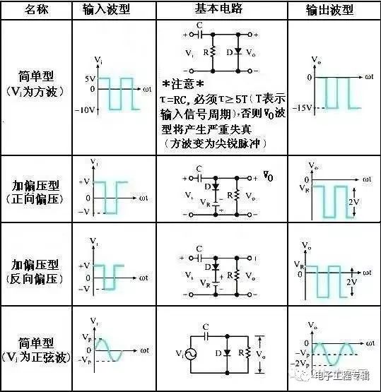
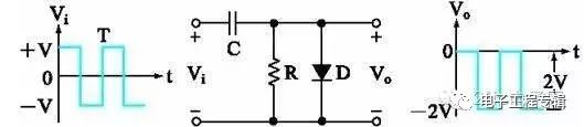
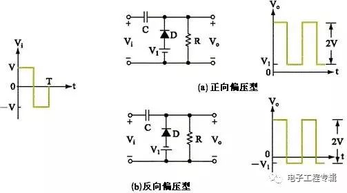
Positive clamp (1) simple type

Working principle Vi is negative for half a week, DON, C is charged to V value (left negative, right positive), Vo = 0V. When Vi is half a week, DOFF, Vo=VC+Vi (positive half cycle) = 2V. (2) biased type
Easy way to judge the output waveform
1. The reference voltage V1 determines the reference point of the output waveform on the coordinate axis. 2. The direction of the diode D determines the direction in which the original waveform moves, if the direction of the diode is
 , the waveform must move up; if the direction of the diode is
  , the waveform must move down.
3 After determining the reference point and direction, and then drawing the original waveform on the output coordinate axis based on the reference point, we are asking for it. Comparison of several diode positive clamp circuits
In 2008,a new industrial park of Liandajin was built in Daya Bay National Economic Development Zone,huizhou with CNY120 million.The Park covers an area of 20000 square meters including 12000 square meters of manufacturing plant,The employees has been up to 1000 and the output has been 60000 square meters per month.
PCB,PCB Manufacturer,PCB Fabricator,Circuit Board,Printed Circuit Board
Huizhou Liandajin Electronic Co., Ltd , https://www.ldjpcb.com