Device connection / reference
This article refers to the address: http://
ADL5375 : 400 MHz to 6 GHz Wideband Quadrature Modulator
ADL5320: 400 MHz to 2700 MHz 1/4 W RF Driver Amplifier
Evaluation and design support
Circuit evaluation board
ADL5375 Evaluation Board (ADL5375-05-EVALZ)
Design and integration files
Schematic, layout file, bill of materials
Circuit function and advantage
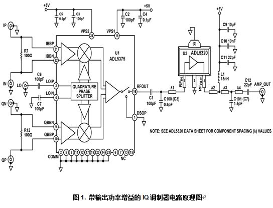
Whether the IQ modulator is used for direct conversion applications or as an upconverter for the first intermediate frequency (IF), there is usually some gain directly applied after the IQ modulator. This article describes how to select the appropriate driver amplifier to provide the first stage gain at the output of the IQ modulator. The device shown in Figure 1 is the ADL5375 IQ modulator and the ADL5320 driver amplifier. Both devices are well matched at the system level; that is, they have the same performance, so neither side will cause overall performance degradation. Because of the good dynamic range matching of these devices, it is recommended to make a simple direct connection between the IQ modulator and the RF driver amplifier without any attenuation between the devices.
Circuit description
The ADL5375 is a general purpose, high performance IQ modulator with an output frequency range of 400 MHz to 6 GHz. With low noise and a wide input baseband bandwidth of 750 MHz (3 dB), the device can be driven with multiple modulation and bandwidth signals. These input signals can be centered on either a DC or a complex intermediate frequency.
The LO interface with the ADL5375 is 1XLO type, that is, the output frequency and the LO frequency are equal (when the baseband signal is centered on DC). Circuit Note CN-0134 describes how to drive the ADL5375 with the ADF4350.
System level calculation and RF amplifier selection
The ADL5375's output compression point (OP1dB) and third-order compression point ( OIP3 ) are around 10 dBm and 25 dBm, respectively, in the frequency range from 1 GHz to 2 GHz. When selecting an RF amplifier to provide gain after the IQ modulator, the device with input P1dB and input IP3 equal to or slightly above these values ​​must be selected. If the input P1dB and input IP3 of the selected device are lower, the cascading performance will be degraded; if these two specifications are significantly higher than the ADL5375, it will not bring any benefits and may cause the total supply current of the signal chain to appear. No need to increase.
The ADL5320 is a driver amplifier (an RF amplifier that requires an external tuning component) and is rated for operation from 400 MHz to 2700 MHz. With a 5 V supply, it consumes 104 mA (it can also be powered from a supply as low as 3.3 V, where power and performance are degraded).
Table 1 shows the specifications for the IP3 (OIP3) and P1dB (OP1dB) of the ADL5375 IQ modulator to the output at 1900 MHz and the ADL5320 driver amplifier to the input. In both cases, the specification of the IQ modulator to the output differs from the specification of the amplifier to the input by about 3 dB.
Table 1. IP3 and P1dB Specifications for ADL5375 IQ Modulators and ADL5320 Driver Amplifiers at 1900 MHz

Figure 2 shows the simulated cascade performance of the IQ modulator and driver amplifier at 2140 MHz. This simulation was done using the ADIsimRF design tool. It is worth noting that the difference between the modulator's OIP3 (24.2 dBm) and the composite OIP3 (36.5 dBm) is just slightly less than the gain of the ADL5320 driver amplifier (13.7 dB). This indicates that the driver amplifier has a very small effect on the overall OIP3.
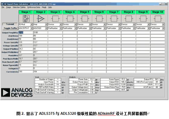
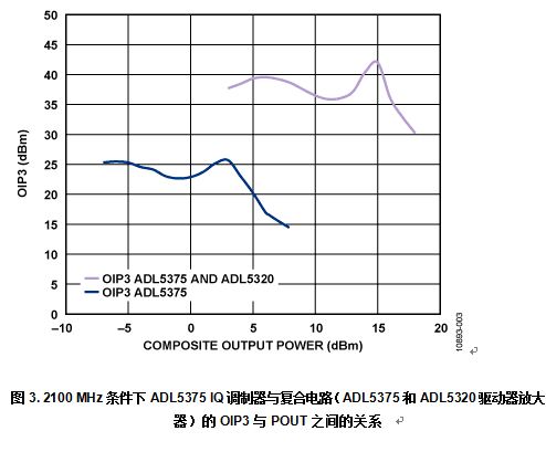
Figure 3 shows the relationship between OIP3 and output power (POUT) measured at the output of the IQ modulator and the output of the composite circuit. The shape of the two OIP3 curve profiles is very similar, with only an offset in output power and OIP3. This further indicates that IP3 will only drop slightly as the signal passes through the RF amplifier.
Select output power level
Although the OIP3 level of the circuit is between 35 dBm and 40 dBm at an output power level of up to 15 dBm, this is not possible in actual operation, especially if the envelope modulation scheme is not constant. Relatively high peak-to-average ratio. To understand this, check the input voltage and output power transfer function of the circuit and then consider the typical drive level at the input of the IQ modulator.
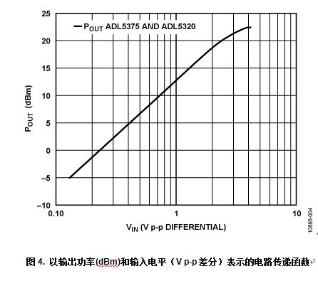
Figure 4 shows the circuit transfer function expressed in terms of output power (dBm) and input voltage (V pp) when using a CW sine wave drive signal. IQ modulators such as the ADL5375 are typically driven by dual-channel, current-output, digital-to-analog converters (DACs). In general, the two current outputs of the DAC (nominally 0 mA to 20 mA) are grounded through two 50 Ω resistors and two 100 Ω shunt resistors are placed on each IQ input (for this interface) For more information, see Circuit Note CN-0205). When the DAC is operating at 0 dBFS, this corresponds to a drive level of 1 V pp or 0.353 V rms on the IQ modulator (the insertion loss of the low-pass filter is ignored here, which is usually placed in the DAC and IQ modulation). Between the devices). This produces an output power of approximately 13 dBm.
Assuming the I and Q inputs of the IQ modulator are terminated by a 100 Ω resistor as described above, the output power curve can be plotted against the dBFS drive level of a typical ADI DAC (see Figure 5). Therefore, the drive level of 0 dBFS corresponds to 1 V pp, which results in the same 13 dBm output power as described above.
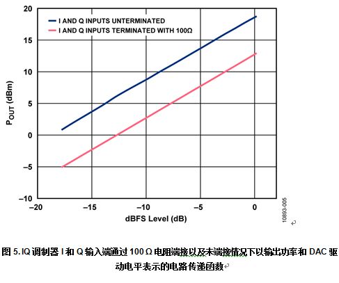
Figure 5 also shows the transfer function of the circuit when the I and Q inputs are not terminated by a 100 Ω resistor. Since the resulting DAC voltage drive level is doubled (up to 2 V pp), the resulting output power is increased by 6 dB relative to the same DAC drive level.
Although the circuit can operate without I and Q termination resistors, this does pose some problems for filters that are typically placed between the DAC and the IQ modulator. Since the filter is typically terminated at both ends, it is best to place some resistance between the I and Q inputs of the IQ modulator (the unterminated input resistance of these inputs is approximately 60 kΩ). Resistance values ​​in the range of 100 Ω to 1000 Ω can be used to increase the resulting DAC voltage drive level and corresponding output power. However, care must be taken when designing the filter between the DAC and the IQ modulator to ensure that it supports different source and load impedances.
As can be seen from Figure 4 and Figure 5, the output power is approximately 13 dBm with a 1 V pp sine wave (0 dBFS) signal (I and Q inputs are terminated by a 100 Ω resistor). In fact, the DAC drive level must be slightly below 0 dBFS to reduce distortion (typically 1 dB to 2 dB). In addition, the rms drive level should also be reduced, the specific amplitude is equal to the peak-to-average ratio of the carrier modulation. The ratio of peak envelope power (PEP) to rms power is typically 5 dB (for a modulation scheme similar to QPSK, 0 dB in the special case of modulation with a constant envelope) to 10 dB (for higher order) The QAM modulation scheme) is within range. Referring to Figure 6, this indicates that an output power level in the range of 0 dBm to 10 dBm is feasible.
The adjacent channel power ratio (ACPR) of single-carrier wideband code division multiple access (WCDMA) signals has become a mainstream indicator for evaluating circuit-level distortion (ie, relative to evaluations that rely solely on IP3 and IMD levels). Figure 6 shows the relationship between the measured circuit ACPR and the output power level. In the case of WCDMA signals, ACPR is defined as the ratio of the power in the carrier (bandwidth of 3.84 MHz) to the power in the adjacent channel (channel spacing is 5 MHz), also measured at 3.84 MHz bandwidth. The curve also shows the phase-to-channel power ratio of the same type of measurement, but with a carrier offset of 10 MHz.
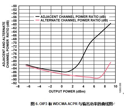
In this example, the ratio of the PEP to the root mean square of the signal is approximately 10 dB (the peak-to-average ratio of the WCDMA signal depends on the configuration and loading mode of the carrier). Select an output power level from 0 dBm to 10 dBm based on the curve and the desired ACPR level. When the power level is below 0 dBm, the ACPR starts to depend on the signal-to-noise ratio of the circuit that is gradually decreasing.
Common changes
The ADL5320 driver amplifier is rated for operation from 400 MHz to 2.7 GHz. This conveniently covers the lower part of the rated frequency range of the ADL5375 IQ modulator. The ADL5321 driver amplifier is recommended for operation in the 2.3 GHz to 4 GHz frequency range. Both the ADL5320 and ADL5321 must be tuned to their respective operating frequency ranges. The data sheets for both devices contain tables that provide recommended values ​​for component tuning for common operating frequencies.
An internally matched wideband gain block such as the ADL5601 or ADL5602 can also be used to provide gain at the output of the IQ modulator. However, because of the low OIP3 of these devices (as opposed to the ADL5320 and ADL5321), they tend to determine the overall IP3 of the circuit and reduce it.
Many narrowband IQ modulators offer higher performance over their operating frequency range. For example, ADL5370/ADL5371/ADL5372/ADL5373/ADL5374. These narrowband devices offer higher gain and OIP3 than the ADL5375. When used with the ADL5320 and ADL5321 driver amplifiers, the end result is a higher total output power, similar to the composite OIP3.
The ADRF6701/ADRF6702/ADRF6703/ADRF6704 family of narrowband IQ modulators integrate a phase-locked loop (PLL) and a voltage controlled oscillator (VCO). The performance of these devices is similar to the ADL5370/ ADL5371/ ADL5372/ ADL5373/ ADL5374 series, but with a higher level of integration.
There are many options for driving the I and Q inputs of the IQ modulator. The AD9125 and AD9122 are 16-bit dual-channel DACs operating at 1 GSPS and 1.2 GSPS, respectively. These devices can be used to generate a baseband spectrum (centered at 0 Hz) or a complex IF spectrum (typically in the 100 MHz to 200 MHz range).
Circuit evaluation and testing
This circuit is implemented using the ADL5375 evaluation board (ADL5375-05-EVALZ) that includes the ADL5320 driver amplifier. This board can be configured to provide an IQ modulator output signal, or a composite modulator and amplifier signal. The default configuration for this board is the modulator and amplifier composite output, and the amplifier is tuned to operate from 1800 MHz to 2200 MHz. As mentioned above, the ADL5320 data sheet provides values ​​and placement locations for capacitive tuning to support other frequencies.
Equipment requirements
The following equipment is required:
The ADL5375 evaluation board ( ADL5375-05-EVALZ)
. ADL5375 Evaluation Board (ADL5375-05-EVALZ)
Two RF signal generators: Agilent 8648C or equivalent operating at 25 MHz and 26 MHz
Two RF signal generators: Agilent 8648C or equivalent, operating at 25 MHz and 26 MHz
A RF signal generator: Agilent 8648C or equivalent operating at approximately 2 GHz
An RF signal generator: Agilent 8648C or equivalent, operating at approximately 2 GHz
A RF spectrum analyzer: Rohde & Schwarz FSIQ, Rohde & Schwarz FSQ, Agilent PSA, or equivalent
An RF spectrum analyzer: Rohde & Schwarz FSIQ, Rohde & Schwarz FSQ, Agilent PSA or equivalent
A ZFSC-2-2-S+ 180° power splitter/combiner, Mini-Circuits
. A ZFSC-2-2-S+ 180° Power Splitter/Synthesizer, Mini-Circuits
A ZMSCQ-2-50+ 90° power splitter, Mini-Circuits
. A ZMSCQ-2-50+ 90° Power Splitter, Mini-Circuits
. Two ADT2-1T 1:2 baluns, Mini-Circuits
. Two ADT2-1T 1:2 Barron, Mini-Circuits
Four ZFBT-6GW-FT+ bias tees, Mini-Circuits
. Four ZFBT-6GW-FT+ Bias, Mini-Circuits
Setup and testing
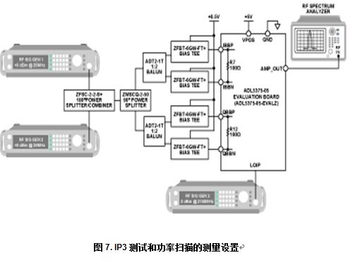
Figure 7 shows the test setup for the IP3 test and the power scan test. The signals generated by two RF signal generators operating at 25 MHz and 26 MHz, respectively, are passively combined by a 180° phase splitter/combiner with good input isolation. The two-tone signal is then applied to a 90° phase splitter that is rated for operation from 25 MHz to 50 MHz. These phase splitter outputs are then applied to two 1:2 transformers to produce a differential output signal (the 0° output of the phase splitter should be passed to the IP and IN inputs of the IQ modulator). These differential signals are then applied to the four biasers to be biased to 0.5 V. The network is terminated by two 100 Ω resistors (pads for these resistors are available on the ADL5375 EV kit).
The local oscillator (LO) of the ADL5375 is provided by a third signal generator, producing 0 dBm. The final output frequency is equal to the difference between the input RF signal frequency and the LO frequency. Therefore, if the frequency of the two-tone signal is 25 MHz and 26 MHz, and the frequency of the LO is 2150 MHz, the output spectrum will appear at 2124 MHz and 2125 MHz.
This circuit can also be implemented using the AD9122 dual DAC evaluation board (AD9122-M5375-EBZ) with the ADL5375 IQ modulator. In this case, the output of the ADL5375 IQ modulator should be connected to a separate ADL5320 evaluation board (ADL5320-EVALZ). The benefit of this approach is that the DAC can generate a properly biased differential signal without the need for a bias, phase splitter, and transformer.
Shenzhen Ever-smart Sensor Technology Co., LTD , https://www.fluhandy.com